This HTML manual corresponds to Magic version 8.3 and technology formats up to and including 35. This manual is equivalent to the manual "Magic Maintainer's Manual #2" that comes with the Magic source distribution. The tutorial "WRL Extentions to the Magic Technology File" has been merged into this document.
Introduction
Downloads and Installation
Command-Line Invocation
Technology File Format Overview
Tech section
Version section
Planes section
Types section
Contact section
Aliases section
Styles section
Compose section
Connect section
Cifoutput section
Cifinput section
Lef section
Mzrouter section
Drc section
Extract section
Wiring section
Router section
Plowing section
Plot section
Conditionals, File Inclusions, and Macro Definitions
Magic Tutorial #1: Getting StartedYou should also read at least the first, and probably all four, of the papers on Magic that appeared in the ACM IEEE 21st Design Automation Conference, and the paper "Magic's Circuit Extractor", which appeared in the ACM IEEE 22nd Design Automation Conference. The overview paper from the DAC was also reprinted in IEEE Design and Test magazine in the February 1985 issue. The circuit extractor paper also appeared in the February 1986 issue of IEEE Design and Test magazine.
Magic Tutorial #2: Basic Painting and Selection
Magic Tutorial #6: Design-Rule Checking
Magic Tutorial #8: Circuit Extraction
Magic Tutorial #9: Format Conversion for CIF and GDS
Commands introduced in this manual:
path, tech, *watch
Macros introduced in this manual:
(None)
Changes since Magic version 7.4:
Changes since Magic version 7.2:
Changes since Magic version 6.5:
Magic is a technology-independent layout editor. All technology-specific information comes from a technology file. This file includes such information as layer types used, electrical connectivity between types, design rules, rules for mask generation, and rules for extracting netlists for circuit simulation.
This manual describes the use, contents, and syntax of Magic's technology file format, and gives hints for building a new one or (more typically) rewriting an existing one for a new fabrication process. References to specific files in the Magic distribution assume that your current working directory is the Magic source top-level directory.
Typically, there is a different technology file for each fabrication process supported by Magic. Scalable technologies, which are (within limits) independent of feature size, will typically have one technology file for all processes supporting the same set of lambda-based (scalable) DRC rules. That said, modern technologies (post-1980's, more or less) tend to be more restrictive in their design rules, and consequently not scalable. This is particularly true of processes which push the envelope on feature sizes.
The Magic source distribution is packaged with a "standard" set of scalable SCMOS rules, which is the technology loaded by default. Default settings are for 1psymm technology, which is out of date. However, the variety and availability of processes means that the "definitive" set of technology files is prohibitively large to be included with the Magic source. In addition, process refinements generally require technology file updates on a regular basis. Because of this, the basic collection of technology files is handled by the MOSIS foundation, not by the Magic development team. This collection represents all processes which are available for fabriction through the MOSIS foundation. Most other vendors have proprietary process specifications, requiring tool maintainers to write their own technology files or modify an existing one to match the proprietary process.
The standard technology file set can be downloaded from an FTP server at the MOSIS foundation. These files are regularly updated, but there is usually a symbolic link called "current" to the most recent stable revision. The download URL is the following:
ftp://ftp.mosis.edu/pub/sondeen/magic/new/beta/current.tar.gz
Assuming that the install destination for magic is /usr/local, this file should be put either in /usr/local/lib/magic/sys or (preferably) in /usr/local/lib/magic/sys/current. Other destinations may be used, if the system search path is appropriately specified on startup (see Section 3, below).
The technology file collection is in tarred, gzipped format, and should be installed with the following commands:
cd /usr/local/lib/magic/sys/current
gunzip current.tar.gz
tar xf current.tar
Once unpacked, these files are ready to be used in Magic.
You can run Magic with a different technology by specifying the -Ttechfile flag on the command line you use to start Magic, where techfile is the name of a file of the form techname.tech, searched for in one of the following directories (listed by search order):
tech load filename -noprompt [-nooverride]
A technology file is organized into sections, each of which begins with a line containing a single keyword and ends with a line containing the single word end. If you examine one of the Magic technology files in the installation directory ${CAD_ROOT}/magic/sys/, e.g., scmos.tech, you can see that it contains the following sections:
tech
version
planes
types
styles
contact
aliases
compose
connect
cifoutput
cifinput
lef
mzrouter
drc
extract
wiring
router
plowing
plot
These sections must appear in this order in all technology files. Every technology file must have all of the sections, although the sections need not have any lines between the section header and the end line.
Historically, technology files were written in a C-language context which was processed by the C preprocessor. This allows the use of C-language comments ("/* ...*/") and the use of preprocessing definitions ("#define ...") and conditionals ("#ifdef ...#endif"). The technology files were generated from a Makefile with the preprocessor constructs used to generate different sections of the technology file at different lambda scales. The decreasing use of scalable processes, however, has made this method largely obsolete, and the standard collection of technology files from MOSIS does not use them at all. Technology files are now written in their final form, not in preprocessed form. Information regarding preprocessor constructs is not included below, but can of course be obtained from the manual pages for the preprocessor itself (gcc or cpp). But also note that the use of C preprocessors for processing text files other than source code is now generally discouraged in favor of using a macro definition processor like m4 (see the manual page for m4 for details). On the other hand, macro definition processors are almost universally despised, so many preprocessor functions have been written into the technology file syntax.
The default scmos set of technology files included with the Magic distribution is still processed via the C preprocessor. Preprocessed files have the extension ".tech.in". Technology files written specifically for Magic version 7.3 tend to make use of additional features of the technology file syntax that subsume most of the functions of the C preprocessor and M4 processor normally used to generate technology files.
Each section in a technology file consists of a series of lines. Each line consists of a series of words, separated by spaces or tabs. If a line ends with the character " ", the " " is ignored and the following newline is treated as an ordinary blank. For example,
width allDiff 2 \
"Diffusion width must be at least 2"
is treated as though it had all appeared on a single line with no intervening " ". On the other hand, for the purposes of tracking errors in technology file input, the technology file parser treats these as separate lines, so that when magic reports an error on a specific line of the technology file, it will agree with the line numbering of the editor used to edit the file.
Comments may be embedded in the technology file. Magic's technology file parser will ignore all text beginning with the character # through the end of the line.
The rest of this part of the manual will describe each of the technology file sections in turn.
Magic stores the technology of a cell in the cell's file on disk. When reading a cell back in to Magic from disk, the cell's technology must match the name of the current technology, which appears as a single word in the tech section of the technology file. See Table 1 for an example.
Historically, most technologies were named scmos, largely for compatibility reasons. Magic version 7.4 has the command option "load -force" to force an attempt to load a layout drawn in one technology into a magic session using a different technology. Thus, the practice of naming all technologies scmos is highly discouraged, and meaningful names (e.g., a foundry process name) should be used.
Versions of magic prior to 7.2 embedded the format version of the technology in the file name, e.g., scmos.tech27. The last format version to use this syntax, 27, is still accepted as a valid filename extension. Many technology files still use this notation, including (at the time of writing) the collection from MOSIS. Now the format is declared inside the tech section.
If the "format version" line is missing, then the version is assumed to be 27. Otherwise, the compatible format version should be stated in this line. Magic version 6.5, 7.0, and 7.1 use format 27. The stable distribution version 7.4 uses format 31. The current stable distribution version 8.5 uses format 35.
version version-stringThe version-string is not used in any meaningful way by Magic but should be used by technology file maintainers as a way to provide version control over technology file modifications.
description description-string [\
more-description]
The description-string is also not used in any meaningful way by Magic but will be printed to the terminal output and in the Technology Manager window display, and should be used as a sanity check on the technology currently in use for a project. The description may contain multiple lines of text if each line up to but not including the last end with a backslash ("\") character.
Both the version and description strings are retained by Magic and may be queried with the command "tech version".
The planes, types, and contact sections are used to define the layers used in the technology. Magic uses a data structure called corner-stitching to represent layouts. Corner-stitching represents mask information as a collection of non-overlapping rectangular tiles. Each tile has a type that corresponds to a single Magic layer. An individual corner-stitched data structure is referred to as a plane.
Magic allows you to see the corner-stitched planes it uses to store a layout. We'll use this facility to see how several corner-stitched planes are used to store the layers of a layout. Enter Magic to edit the cell maint2a. Type the command *watch active demo. You are now looking at the active plane. Each of the boxes outlined in black is a tile. (The arrows are stitches, but are unimportant to this discussion.) You can see that some tiles contain layers (polysilicon, ndiffusion, ndcontact, polycontact, and ntransistor), while others contain empty space. Corner-stitching is unusual in that it represents empty space explicitly. Each tile contains exactly one type of material, or space.
You have probably noticed that metal1 does not seem to have a tile associated with it, but instead appears right in the middle of a space tile. This is because metal1 is stored on a different plane, the metal1 plane. Type the command :*watch metal1 demo. Now you can see that there are metal1 tiles, but the polysilicon, diffusion, and transistor tiles have disappeared. The two contacts, polycontact and ndcontact, still appear to be tiles.
The reason Magic uses several planes to store mask information is that corner-stitching can only represent non-overlapping rectangles. If a layout were to consist of only a single layer, such as polysilicon, then only two types of tiles would be necessary: polysilicon and space. As more layers are added, overlaps can be represented by creating a special tile type for each kind of overlap area. For example, when polysilicon overlaps ndiffusion, the overlap area is marked with the tile type ntransistor.
Although some overlaps correspond to actual electrical constructs (e.g., transistors), other overlaps have little electrical significance. For example, metal1 can overlap polysilicon without changing the connectivity of the circuit or creating any new devices. The only consequence of the overlap is possibly a change in parasitic capacitance. To create new tile types for all possible overlapping combinations of metal1 with polysilicon, diffusion, transistors, etc. would be wasteful, since these new overlapping combinations would have no electrical significance.
Instead, Magic partitions the layers into separate planes. Layers whose overlaps have electrical significance must be stored in a single plane. For example, polysilicon, diffusion, and their overlaps (transistors) are all stored in the active plane. Metal1 does not interact with any of these tile types, so it is stored in its own plane, the metal1 plane. Similarly, in the scmos technology, metal2 doesn't interact with either metal1 or the active layers, so is stored in yet another plane, metal2.
Contacts between layers in one plane and layers in another are a special case and are represented on both planes. This explains why the pcontact and ndcontact tiles appeared on both the active plane and on the metal1 plane. Later in this section, when the contacts section of the technology file is introduced, we'll see how to define contacts and the layers they connect.
The planes section of the technology file specifies how many planes will be used to store tiles in a given technology, and gives each plane a name. Each line in this section defines a plane by giving a comma-separated list of the names by which it is known. Any name may be used in referring to the plane in later sections, or in commands like the *watch command indicated in the tutorial above. Table 2 gives the planes section from the scmos technology file.
Magic uses a number other planes internally. The subcell plane is used for storing cell instances rather than storing mask layers. The designRuleCheck and designRuleError planes are used by the design rule checker to store areas to be re-verified, and areas containing design rule violations, respectively. Finally, the mhint, fhint, and rhint planes are used for by the interactive router (the iroute command) for designer-specified graphic hints.
There is a limit on the maximum number of planes in a technology, including the internal planes. This limit is currently 64. To increase the limit, it is necessary to change MAXPLANES in the file database/database.h.in and then recompile all of Magic as described in "Maintainer's Manual #1". Each additional plane involves additional storage space in every cell and some additional processing time for searches, so we recommend that you keep the number of planes as small as you can do cleanly.
[-]plane names
Each type defined in this section is allowed to appear on exactly one of the planes defined in the planes section, namely that given by the plane field above. For contacts types such as pcontact, the plane listed is considered to be the contact's home plane; in Magic 7.3 this is a largely irrelevant distinction. However, it is preferable to maintain a standard of listing the lowest plane connected to a contact as it's "home plane" (as they appear in the table).
The minus sign ("-") in front of the plane name is a special convention introduced in Magic version 7.5, that causes layers to be "locked" on startup. A locked layer cannot have its paint geometry changed. This is a useful feature for locking down part of a design, such as a sea-of-gates design where planes below some designated metal layer are prefabricated and cannot be changed. Layer locking prevents inadvertent changes to these layers. Layer locking and unlocking can also be done from the command-line or a startup script, which is probably more useful for a per-design specification of locked layers.
The names field is a comma-separated list of names. The first name in the list is the "long" name for the type; it appears in the .mag file and whenever error messages involving that type are printed. Any unique abbreviation of any of a type's names is sufficient to refer to that type, both from within the technology file and in any commands such as paint or erase.
Magic has certain built-in types as shown in Table 4. Empty space (space) is special in that it can appear on any plane. The types error_p, error_s, and error_ps record design rule violations. The types checkpaint and checksubcell record areas still to be design-rule checked. Types magnet, fence, and rotate are the types used by designers to indicate hints for the irouter.
There is a limit on the maximum number of types in a technology, including all the built-in types. Currently, the limit is 256 tile types. To increase the limit, you'll have to change the value of TT_MAXTYPES in the file database/database.h.in and then recompile all of Magic as described in "Maintainer's Manual #1". Because there are a number of tables whose size is determined by the square of TT_MAXTYPES, it is very expensive to increase TT_MAXTYPES. Magic version 7.2 greatly reduced the number of these tables, so the problem is not as bad as it once was. Most internal tables depend on a bitmask of types, the consequence of which is that the internal memory usage greatly increases whenever TT_MAXTYPES exceeds a factor of 32 (the size of an integer, on 32-bit systems). Magic version 7.3 further alleviates the problem by reducing the number of "derived" tile types that magic generates internally, so that the total number of types is not much larger than the number declared in the types section. Magic-7.4 only generates extra types for pairs of stackable contact types. For a typical process, the number of these derived stacked contact pairs is around 15 to 20.
The declaration of tile types may be followed by a block of alias declarations. This is similar to the "macro" definitions used by preprocessors, except that the definitions are not only significant to the technology file parser, but extend to the user as well. Thus the statement "alias metalstack m1,m2,m3" may be a convenient shorthand where metal layers 1, 2, and 3 appear simultaneously, but the end-user can type the command "paint metalstack" and get the expected result of all three metal layers painted. The alias statement has the additional function of allowing backward-compatibility for technology files making use of stackable contacts (see below) with older layouts, and cross-compatibility between similar technologies that may have slight differences in layer names.
Important: The alias declarations in the types section are allowed for backwards compatibility. However, it should be noted that since contacts are not defined until after the "types" section, the wildcard character "*" cannot be used in alias defitions that appear in the "types" section. If you want to use the wildcard definitions, put all aliases into the (separate) "alias" section (see below).
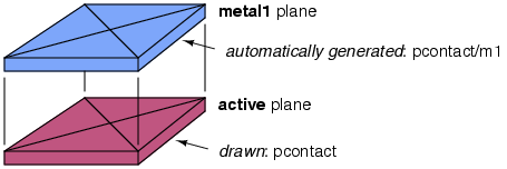
Each line in the contact section begins with a tile type, base, which is thereby defined to be a contact. This type is also referred to as a contact's base type. The remainder of each line is a list of non-contact tile types that are connected by the contact. These tile types are referred to as the residues of the contact, and are the layers that would be present if there were no electrical connection (i.e., no via hole). In Table 5, for example, the type pcontact is the base type of a contact connecting the residue layers polysilicon on the active plane with metal1 on the metal1 plane.
In Magic-7.3 and above, any number of types can be connected, and those types may exist on any planes. It is the duty of the technology file developer to ensure that these connections make sense, especially if the planes are not contiguous. However, because Magic-7.3 handles stacked contacts explicitly, it is generally better to define contacts only between two adjacent planes, and use the stackable keyword (see below) to allow types to be stacked upon one another. The multiple-plane representation exists for backward compatibility with technology files written for versions of Magic prior to 7.3. Stackable contacts in older technology files take the form:
contact pc polysilicon metal1
contact m2c metal1 metal2
contact pm12c polysilicon metal1 metal2
In Magic version 7.3, the above line would be represented as:
contact pc polysilicon metal1
contact m2c metal1 metal2
stackable pc m2c pm12c
where the third line declares that contact types m2c and pc may be stacked together, and that type name "pm12c" is a valid alias for the combination of "pc" and "m2c".
Each contact has an image on all the planes it connects. Figure 1 depicts the situation graphically. In later sections of the technology file, it is sometimes useful to refer separately to the various images of contact. A special notation using a slash character ("/") is used for this. If a tile type aaa/bbb is specified in the technology file, this refers to the image of contact aaa on plane bbb. For example, pcontact/metal1 refers to the image of the pcontact that lies on the metal1 plane, and pcontact/active refers to the image on the active plane, which is the same as pcontact.
 |
In several places in the technology file you'll need to specify groups of tile types. For example, in the connect section you'll specify groups of tiles that are mutually connected. These are called type-lists and there are several ways to specify them. The simplest form for a type-list is a comma-separated list of tile types, for example
poly,ndiff,pcontact,ndc
The null list (no tiles at all) is indicated by zero, i.e.,
0
There must not be any spaces in the type-list. Type-lists may also use tildes ("~") to select all tiles but a specified set, and parentheses for grouping. For example,
~(pcontact,ndc)
selects all tile types but pcontact and ndc. When a contact name appears in a type-list, it selects all images of the contact unless a "/" is used to indicate a particular one. The example above will not select any of the images of pcontact or ndc. Slashes can also be used in conjunction with parentheses and tildes. For example,
~(pcontact,ndc)/active,metal1
selects all of the tile types on the active plane except for pcontact and ndc, and also selects metal1. Tildes have higher operator precedence than slashes, and commas have lowest precedence of all.
A special notation using the asterisk ("*") is a convenient way to abbreviate the common situation where a rule requires the inclusion of a tile type and also all contacts that define that tile type as one of their residue layers, a common occurrence. The notation
*metal1
expands to metal1 plus all of the contact types associated with metal1, such as ndc, pdc, nsc, m2c, and so forth.
Note: in the CIF sections of the technology file, only simple comma-separated names are permitted; tildes and parentheses are not understood. However, everywhere else in the technology file the full generality can be used. The "*" notation for inclusion of contact residues may be present in any section.
Because the "alias" statement in the "types" section is disallowed from containing wildcard characters, a separate section has been added to the technology file (starting from Magic version 7.5.56), allowing aliases to be defined after the "contacts" section has been declared, and therefore able to use both the "*" wildcard character and the stacked contact alias names defined in the "contacts" section. The syntax is as follows:
alias_name type_listThe alias_name can be any valid name but must be unique (i.e., it cannot shadow an existing type name). The type_list is a comma-separated list of types that may contain contact names, contact aliases, the "*" wildcard character, or any other valid notation for a type list. It may also contain other alias names provided that they are defined before they are used.
Once defined, alias names may be used anywhere in the technology file, and they may be used in commands from the command line.
Magic can be run on several different types of graphical displays. Although it would have been possible to incorporate display-specific information into the technology file, a different technology file would have been required for each display type. Instead, the technology file gives one or more display-independent styles for each type that is to be displayed, and uses a per-display-type styles file to map to colors and stipplings specific to the display being used. The styles file is described in Magic Maintainer's Manual #3: "Styles and Colors", so we will not describe it further here.
Table 6 shows part of the styles section from the scmos technology file. The first line specifies the type of style file for use with this technology, which in this example is mos. Each subsequent line consists of a tile type and a style number (an integer between 1 and 63). The style number is nothing more than a reference between the technology file and the styles file. Notice that a given tile type can have several styles (e.g., pcontact uses styles #1, #20, and #32), and that a given style may be used to display several different tiles (e.g., style #2 is used in ndiff and ndcontact). If a tile type should not be displayed, it has no entry in the styles section.
It is no longer necessary to have one style per line, a restriction of format 27 and earlier. Multiple styles for a tile type can be placed on the same line, separated by spaces. Styles may be specified by number, or by the "long name" in the style file.
The semantics of Magic's paint operation are defined by a collection of rules of the form, "given material HAVE on plane PLANE, if we paint PAINT, then we get Z", plus a similar set of rules for the erase operation. The default paint and erase rules are simple. Assume that we are given material HAVE on plane PLANE, and are painting or erasing material PAINT.
These rules apply for contacts as well. Painting the base type of a contact paints the base type on its home plane, and each image type on its home plane. Erasing the base type of a contact erases both the base type and the image types.
It is sometimes desirable for certain tile types to behave as though they were "composed" of other, more fundamental ones. For example, painting poly over ndiffusion in scmos produces ntransistor, instead of ndiffusion. Also, painting either poly or ndiffusion over ntransistor leaves ntransistor, erasing poly from ntransistor leaves ndiffusion, and erasing ndiffusion leaves poly. The semantics for ntransistor are a result of the following rule in the compose section of the scmos technology file:
compose ntransistor poly ndiff
Sometimes, not all of the "component" layers of a type are layers known to magic. As an example, in the nmos technology, there are two types of transistors: enhancement-fet and depletion-fet. Although both contain polysilicon and diffusion, depletion-fet can be thought of as also containing implant, which is not a tile type. So while we can't construct depletion-fet by painting poly and then diffusion, we'd still like it to behave as though it contained both materials. Painting poly or diffusion over a depletion-fet should not change it, and erasing either poly or diffusion should give the other. These semantics are the result of the following rule:
decompose dfet poly diff
The general syntax of both types of composition rules, compose and decompose, is:
compose type a1 b1 a2 b2 ...
decompose type a1 b1 a2 b2 ...
The idea is that each of the pairs a1 b1, a2 b2, etc comprise type. In the case of a compose rule, painting any a atop its corresponding b will give type, as well as vice-versa. In both compose and decompose rules, erasing a from type gives b, erasing b from type gives a, and painting either a or b over type leaves type unchanged.
|
Contacts are implicitly composed of their component types, so the result obtained when painting a type PAINT over a contact type CONTACT will by default depend only on the component types of CONTACT. If painting PAINT doesn't affect the component types of the contact, then it is considered not to affect the contact itself either. If painting PAINT does affect any of the component types, then the result is as though the contact had been replaced by its component types in the layout before type PAINT was painted. Similar rules hold for erasing.
A pcontact has component types poly and metal1. Since painting poly doesn't affect either poly or metal1, it doesn't affect a pcontact either. Painting ndiffusion does affect poly: it turns it into an ntransistor. Hence, painting ndiffusion over a pcontact breaks up the contact, leaving ntransistor on the active plane and metal1 on the metal1 plane.
The compose and decompose rules are normally sufficient to specify the desired semantics of painting or erasing. In unusual cases, however, it may be necessary to provide Magic with explicit paint or erase rules. For example, to specify that painting pwell over pdiffusion switches its type to ndiffusion, the technology file contains the rule:
paint pdiffusion pwell ndiffusion
This rule could not have been written as a decompose rule; erasing ndiffusion from pwell does not yield pdiffusion, nor does erasing pdiffusion from ndiffusion yield pwell. The general syntax for these explicit rules is:
paint have t result [p]
erase have t result [p]
Here, have is the type already present, on plane p if it is specified; otherwise, on the home plane of have. Type t is being painted or erased, and the result is type result. Table 7 gives the compose section for scmos.
It's easiest to think of the paint and erase rules as being built up in four passes. The first pass generates the default rules for all non-contact types, and the second pass replaces these as specified by the compose, decompose, etc. rules, also for non-contact types. At this point, the behavior of the component types of contacts has been completely determined, so the third pass can generate the default rules for all contact types, and the fourth pass can modify these as per any compose, etc. rules for contacts.
For circuit extraction, routing, and some of the net-list operations, Magic needs to know what types are electrically connected. Magic's model of electrical connectivity used is based on signal propagation. Two types should be marked as connected if a signal will always pass between the two types, in either direction. For the most part, this will mean that all non-space types within a plane should be marked as connected. The exceptions to this rule are devices (transistors). A transistor should be considered electrically connected to adjacent polysilicon, but not to adjacent diffusion. This models the fact that polysilicon connects to the gate of the transistor, but that the transistor acts as a switch between the diffusion areas on either side of the channel of the transistor.
The lines in the connect section of a technology file, as shown in Table 8, each contain a pair of type-lists in the format described in Section 8. Each type in the first list connects to each type in the second list. This does not imply that the types in the first list are themselves connected to each other, or that the types in the second list are connected to each other.
| ||||||||||||||||||||||||||||||||||||||||||
Because connectivity is a symmetric relationship, only one of the two possible orders of two tile types need be specified. Tiles of the same type are always considered to be connected. Contacts are treated specially; they should be specified as connecting to material in all planes spanned by the contact. For example, pcontact is shown as connecting to several types in the active plane, as well as several types in the metal1 plane. The connectivity of a contact should usually be that of its component types, so pcontact should connect to everything connected to poly, and to everything connected to metal1.
The layers stored by Magic do not always correspond to physical mask layers. For example, there is no physical layer corresponding to (the scmos technology file layer) ntransistor; instead, the actual circuit must be built up by overlapping poly and diffusion over pwell. When writing CIF (Caltech Intermediate Form) or Calma GDS-II files, Magic generates the actual geometries that will appear on the masks used to fabricate the circuit. The cifoutput section of the technology file describes how to generate mask layers from Magic's abstract layers.
|
From the 1990's, the CIF format has largely been replaced by the GDS format. However, they describe the same layout geometry, and the formats are similar enough that magic makes use of the CIF generation code as the basis for the GDS write routines. The technology file also uses CIF layer declarations as the basis for GDS output. So even a technology file that only expects to generate GDS output needs a "cifoutput" section declaring CIF layer names. If only GDS output is required, these names may be longer and therefore more descriptive than allowed by CIF format syntax.
The technology file can contain several different specifications of how to generate CIF. Each of these is called a CIF style. Different styles may be used for fabrication at different feature sizes, or for totally different purposes. For example, some of the Magic technology files contain a style "plot" that generates CIF pseudo-layers that have exactly the same shapes as the Magic layers. This style is used for generating plots that look just like what appears on the color display; it makes no sense for fabrication. Lines of the form
style name
are used to end the description of the previous style and start the description of a new style. The Magic command cif ostyle name is typed by users to change the current style used for output. The first style in the technology file is used by default for CIF output if the designer doesn't issue a cif style command. If the first line of the cifoutput section isn't a style line, then Magic uses an initial style name of default.
Each style must contain a line of the form
scalefactor scale [nanometers|angstroms]
that tells how to scale Magic coordinates into CIF coordinates, and how values in the cifoutput layer generation recipes are specified. The argument scale indicates how many hundredths of a micron (centimicrons) correspond to one Magic unit. scale may be any number, including decimals. However, all units in the style description must be integer. Because deep submicron processes may require CIF operations in units of less than one centimicron, the optional parameter nanometers declares that all units (including the scale parameter) are measured in units of nanometers. Likewise, the units may all be specified in angstroms. However unlikely the dimensions may seem, the problem is that magic needs to place some objects, like contacts, on half-lambda positions to ensure correct overlap of contact cuts between subcells. A feature size such as, for example, 45 nanometers, has a half-lambda value of 22.5 nanometers. Since this is not an integer, magic will complain about this scalefactor. This is true even if the process doesn't allow sub-nanometer coordinates, and magic uses the squares-grid statement to enforce this restriction. In such a case, it is necessary to declare a scalefactor of 450 angstroms rather than 45 nanometers (also see the units keyword, below).
Versions of magic prior to 7.1 allowed an optional second (integer) parameter, reducer, or the keyword calmaonly. The use of reducer is integral to CIF output, which uses the value to ensure that output values are reduced to the smallest common denominator. For example, if all CIF values are divisible by 100, then the reducer is set to 100 and all output values are divided by the same factor, thus reducing the size of the CIF output file. Now the reducer is calculated automatically, avoiding any problems resulting from an incorrectly specified reducer value, and any value found after scale is ignored. The calmaonly keyword specified that the scale was an odd integer. This limitation has been removed, so any such keyword is ignored, and correct output may be generated for either CIF or Calma at all output scales.
All values written to CIF files are in units of centimicrons, and finer resolution is obtained by using the CIF numerator and denominator scaling as needed. GDS (Calma) files do not have adjustible scaling like CIF files do, so if the units are specified in angstroms in the scalefactor line, then it is also necessary to specify the GDS units as angstroms as well, which can be done with the units command. This command sets the resolution used for GDS output values.
units angstroms
In addition to specifying a scale factor, each style can specify the size in which chunks will be processed when generating CIF hierarchically. This is particularly important when the average design size is much larger than the maximum bloat or shrink (e.g, more than 3 orders of magnitude difference). The step size is specified by a line of the following form:
stepsize stepsize
where stepsize is in Magic units. For example, if you plan to generate CIF for designs that will typically be 100,000 Magic units on a side, it might make sense for stepsize to be 10000 or more.
Each style can specify the minimum grid spacing on which a process will allow geometry to be generated. By default, there is no limit. When a limit is set, Magic cannot rescale its internal grid to a value that is either lower than, or not a multiple of, the grid limit. Normally, when geometry read from a CIF, GDS, or database file is smaller than the internal grid, magic rescales its grid to accomodate the input. The gridlimit sets a limit on how much the grid can be scaled down to avoid the possibility of Magic being able go generate CIF or GDS output that is off-grid. The grid limit is specified by a line of the following form:
gridlimit value
where the value is in the same units as other dimensions in the definition for the style (i.e., centimicrons, nanometers or angstroms, the first being the default and the others specified in the scalefactor statement).
Finally, each style can specify several options affecting the behavior of the output. Currently, there are two options available. These may be specified one at a time, or all in the same statement, with options separated by space.
options calma-permissive-labels
options grow-euclidean
The option "grow-euclidean" changes the algorithm for the "grow" and "shrink" operations. With this option set, non-Manhattan edges are grown to the minimum amount necessary to satisfy the grow amount while still having corner points land on-grid. When this option is not set, non-Manhattan edges are expanded (or shrunk) in both directions by the amount specified. This allows all tiles to be grown or shrunk independently of each other, leading to a much simpler and faster algorithm.
Magic version 8.0 defines a few more options, as follows:
options see-no-vendor
options no-errors
The "no-errors" option will prevent errors from being reported and displayed as feedback regions during "cif see" or "cif paint" commands. It is generally not recommended for output styles used for generating actual output, as it would then hide errors from the user. It is useful in certain applications, as when the "squares" operator is used to create fill patterns with the "cif paint" command. Areas too small to place paint will not generate error messages and feedback regions.
The main body of information for each CIF style is a set of layer descriptions. Each layer description consists of one or more operations describing how to generate the CIF for a single layer. The first line of each description is one of
layer name [layers]
templayer name [layers]
labellayer name [layers]
These statements are identical, except that templayers are not output in the CIF file. They are used only to build up intermediate results used in generating the "real" layers. In each case, name is the CIF name to be used for the layer. If layers is specified, it consists of a comma-separated list of Magic layers and previously-defined CIF layers in this style; these layers form the initial contents of the new CIF layer (note: the layer lists in this section are less general than what was described in Section 8; tildes and parentheses are not allowed). If layers is not specified, then the new CIF layer is initially empty. The following statements are used to modify the contents of a CIF layer before it is output.
The labellayer is similar to layer in that it generates output directly to the GDS file, but it is used to automatically generate label text, such as when a specific identifying text is required on a layer. For example, a specific FET type like an ESD FET may be distinguishable only by a label tagging the device. For each individual tile generated for the label layer, a label will be added to the GDS output file. The text of the label will be the name name of the label layer, and the position of the label will be centered on the tile. There is no associated "attachment" geometry associated with the label other than the position.
After the layer or templayer statement come several statements specifying geometrical operations to apply in building the CIF layer. Each statement takes the current contents of the layer, applies some operation to it, and produces the new contents of the layer. The last geometrical operation for the layer determines what is actually output in the CIF file. The most common geometrical operations are:
or layers
and layers
and-not layers
grow amount
shrink amount
bloat-or layers layers2 amount layers2 amount ...
squares size
squares border size separation
Some more obscure operations are:
bloat-max layers layers2 amount layers2 amount ...
bloat-min layers layers2 amount layers2 amount ...
bloat-all layers layers2 [distance]
close area
bridge spacing width
grow-grid amount
grow-min amount
maxrect name internal|external
interacting layers
noninteracting layers
overlapping layers
nonoverlapping layers
orthogonal [fill|remove]
net name layers
mask-hints name
squares-grid border size separation x y
slots border size separation
slots border size separation border_long
slots border size separation border_long size_long sep_long [offset [start]]]
bbox [top]
tagged text [layers]
The operation or takes all the layers (which may be either Magic layers or previously-defined CIF layers), and or's them with the material already in the CIF layer. The operation and is similar to or, except that it and's the layers with the material in the CIF layer (in other words, any CIF material that doesn't lie under material in layers is removed from the CIF layer). And-not finds all areas covered by layers and erases current CIF material from those areas. Grow and shrink will uniformly grow or shrink the current CIF layer by amount units, where amount is specified in CIF units, not Magic units. The grow-grid operator grows layers non-uniformly to snap to the grid spacing indicated by amount. This can be used to ensure that features fall on a required minimum grid. The grow-min operator looks for geometry where the width or height is less than amount, and expands in that direction to ensure that no dimension of the geometry is less than amount.
The three "bloat" operations bloat-or, bloat-min, and bloat-max, provide selective forms of growing. In these statements, all the layers must be Magic layers. Each operation examines all the tiles in layers, and grows the tiles by a different distance on each side, depending on the rest of the line. Each pair layers2 amount specifies some tile types and a distance (in CIF units). Where a tile of type layers abuts a tile of type layers2, the first tile is grown on that side by amount. The result is or'ed with the current contents of the CIF plane. The layer "*" may be used as layers2 to indicate all tile types. Where tiles only have a single type of neighbor on each side, all three forms of bloat are identical. Where the neighbors are different, the three forms are slightly different, as illustrated in Figure 12.3. Note: all the layers specified in any given bloat operation must lie on a single Magic plane. For bloat-or all distances must be positive. In bloat-max and bloat-min the distances may be negative to provide a selective form of shrinking.
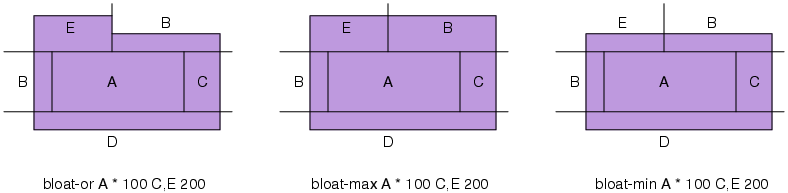 |
In retrospect, it's not clear that bloat-max and bloat-min are very useful operations. The problem is that they operate on tiles, not regions. This can cause unexpected behavior on concave regions. For example, if the region being bloated is in the shape of a "T", a single bloat factor will be applied to the underside of the horizontal bar. If you use bloat-max or bloat-min, you should probably specify design-rules that require the shapes being bloated to be convex.
The fourth bloat operation bloat-all takes all tiles of
types layers, and grows to include all neighboring tiles of
types layers2. This is very useful to generate marker layers
or implant layers for specific devices, where the marker or implant must
cover both the device and its contacts. Take the material of the device
and use bloat-all to expand into the contact areas.
From magic version 8.2.146, layers and layers2 may be in
different and non-overlapping planes. In effect, this creates a way of
using one layer (layers) to tag another layer (layers2).
Note that if the planes of layers and layers2 are disjoint,
then output is only generated for layers2. This method is useful,
for example, for marking a well as a high-voltage well due to the
presence of high-voltage diffusion in it, without having to declare a
separate layer type for a high-voltage well.
From magic version 8.2.148 layers may contain one or more CIF layers
in addition to magic layers. This allows tagging of geometry that is within
the boundary of an area derived from other layers using the CIF boolean operators.
From magic version 8.3.16, layers2 may contain one or more CIF temp layers.
The restriction is that layers2 must contain either all magic layers
or all CIF temp layers. In general, only one CIF temp layer will be specified;
if more than one temp layer is present, then the effect will be to grow to cover
the area of the union (OR) of all the temp layers in layers2.
From magic version 8.3.508, the additional distance value limits the
distance of the expansion. This is mostly useful for generating temporary
layers for DRC checks (in particular for latch-up rules) in conjunction with
the "DRC CIF" rules. However, it has other uses, such as allowing "space"
to be used in the layers2 argument without causing unbounded
expansion to infinity. The rule with distance is defined as an
expansion of the area of each tile of type layers to the edge of
adjoining or underlapping tiles of type layers2 or to a maximum
distance of distance from the edge of the tile of type layers.
Please note that "bloat-all distance" is extremely compute-intensive. In cases where layers are very common layers and/or distance is large, using this function may be prohibitive. An alternative is to use a stepped series of grow and and (or and-not) operations to expand one layer into another. This works as long as the grow distance for each step is not so large that it might "reach across" a space and catch material on the other side. This can make such stepped series very long, with scores of iterations. This is, surprisingly, much faster to compute than bloat-all distance. Since scores of repeated lines in the tech file is tedious and difficult to understand at a glance, a general-purpose tech file command repeat was added in magic version 8.3.612. The repeat statement is not an operator but can be used anywhere in a tech file. But its usefulness is limited to stepped series of CIF output operators, which is why it is mentioned here.
repeat steps
...
endrepeat
The close operator handles DRC rules of the form "minimum enclosed area
of layer must be at least width X", where the dimension in question is a hole
in a material layer rather than the material itself. The rule acts on the
existing generated plane (like grow and shrink operators). It
takes one argument area, which is the minimum allowed enclosed area
in the material, in units of distance squared. The plane of material is
searched for enclosed holes with area less than area, which are then
filled in with the material to close the gap and satisfy the rule.
Note that close is different
from the use of "grow" followed by a "shrink" of the same
amount. That may work under most circumstances to fill small holes in the
material. However, in some cases the minimum hole size is larger than the
material spacing rule, and the grow/shrink pair of operators can then merge
across areas where the material is prohibited. Using the close
operator is much simpler than finding all the ways the grow/shrink operation
can fail and eliminating them with complicated additional operations.
The bridge operator handles problems which arise from the use of "grow" followed by "shrink" of the same amount. That method works in most cases to close up narrow gaps between unconnected parts of a layer (typically an automatically generated implant layer). However, it will fail for geometry in a catecorner arrangement, either not closing the gap at all, or else generating a small sliver; a DRC width error or a DRC spacing error results. By putting the bridge operator ahead of the grow-shrink pair, additional material is added in the corner areas between shapes to resolve the width and spacing errors, resulting in a clean layout. The argument spacing is the minimum spacing distance for the layer, and width is the minimum width of the layer. The bridge operator was introduced in magic version 8.3.24.
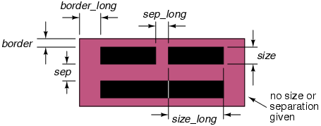
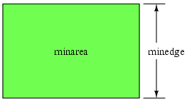
An important geometric operation for creating contact cuts is squares. It examines each tile on the CIF plane, and replaces that tile with one or more squares of material. Each square is size CIF units across, and squares are separated by separation units. A border of at least border units is left around the edge of the original tile, if possible. This operation is used to generate contact vias, as in Figure 3. If only one argument is given in the squares statement, then separation defaults to size and border defaults to size/2. If a tile doesn't hold an integral number of squares, extra space is left around the edges of the tile and the squares are centered in the tile. If the tile is so small that not even a single square can fit and still leave enough border, then the border is reduced. If a square won't fit in the tile, even with no border, then no material is generated. The squares operation must be used with some care, in conjunction with the design rules. For example, if there are several adjacent skinny tiles, there may not be enough room in any of the tiles for a square, so no material will be generated at all. Whenever you use the squares operator, you should use design rules to prohibit adjacent contact tiles, and you should always use the no_overlap rule to prevent unpleasant hierarchical interactions. The problems with hierarchy are discussed in Section 12.6 below, and design rules are discussed in Section 15.
Magic version 7.5.159 introduced a new algorithm for generating contact cuts. This algorithm is area-based, not tile-based, and so does not suffer many of the restrictions of the original algorithm. Hierarchical overlap is guaranteed with exact_overlap (rather than the much more restrictive no_overlap rule), and it is not necessary to restrict contacts to be rectangles using the rect_only DRC rule. Contact areas may form any arbitrary geometry, including octagonal areas (often used for pads), or guard rings (which may intersect). This algorithm covers both the squares and squares-grid (see below) operators.
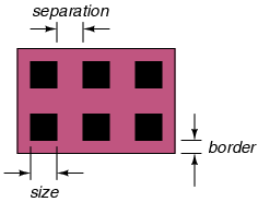 |
The squares-grid operator is similar to squares and takes the same arguments, except for the additional optional x and y offsets (which default to 1). Where the squares operator places contacts on the half-lambda grid, the squares-grid operator places contacts on an integer grid of x and y. This is helpful where manufacturing grid limitations do not allow half-lambda coordinates. However, it is necessary then to enforce a "no-overlap" rule for contacts in the DRC section to prevent incorrect contacts cuts from being generated in overlapping subcells. The squares-grid operator can also be used with x and y values to generate fill geometry, or to generate offset contact cut arrays for pad vias.
The slots operator is similar to squares operator, but as the name implies, the resulting shapes generated are rectangular, not (necessarily) square. Slots are generated inside individual tiles, like the squares operator, so each slots operation is separately oriented relative to the tile's long and short edges. Separate border, size, and separation values can be specified for the short and long dimensions of the tile. This operator can be used in a number of situations:
Note that the slots operator comes in three different forms with different numbers of arguments. With only three arguments (short side description only), the slots operator creates stripes that extend to the edge of the tile. With four arguments (short side description plus long side border dimension only), the slots operator create stripes that extend to the edge of the tile, with an appropriate border spacing at each end. In these two cases, the slots have variable length that is set by the size of the tile. In the final form, all short and long side dimensions are declared. The generated slots are of fixed size, and like the squares operator, their positions will be adjusted to center them on the tile.
The offset lets each row of slots be offset from the previous one by a fixed amount (in the horizontal direction only). This is intended to produce offset patterns as often required for fill shapes. It works best in conjunction with the "bbox top" operator, such that the slots generator operates over a single, uninterrupted rectangular area. Generate a full pattern over the whole area, then cut to size to avoid existing layer obstructions, then shrink and grow to remove shapes that have been partially cut. If different layers need to be offset with respect to each other, use the additional start argument (default zero) to generate an additional offset a distance start in both horizontal and vertical directions from the lower left corner of the area to fill.
The offset parameter was implemented in magic version 8.2.165.
The bbox operator generates a single rectangle that encompasses the bounding box of the cell. This is useful for the occasional process that requires marker or implant layers covering an entire design. The variant bbox top will generate a rectangle encompassing the bounding box of the cell, but will only do so for the top-level cell of the design.
The net operator introduced in Magic 8.0 is a connectivity-based operator. It will search for the network node named "name" (which may be a hierarchical name), and select all paint in that network that matches any layers in the list layers. The same restrictions for node name searches applies as for the "goto" command. Multiple nodes with the same label will be ignored unless those nodes are marked as ports (see the "port" command). Normally, the net operator is used with globally-defined node names to find known power and ground buses.
The mask-hints operator was introduced in Magic 8.3.97. It is a way to work around the general problem that automatic generation of mask layers can be very tricky in spite of the many methods used to avoid DRC errors in the output generation. One way to handle this is to introduce mask layers into the layer types in the techfile. That requires reserving additional types in the mask, and a complete setup in the techfile with layer styles and other handling, for something that is rarely used. The mask-hints operator is a simpler method, by which mask layers can be specified with a string of coordinate pairs in a cell property (see the property command). The argument name can be any name, although for clarity it is helpful to set this to the name of a GDS mask layer. The mask-hints operator does not do any layer manipulations itself. Rather, it enables the output generator to look for mask hints in the properties of every cell (see the property command). The property string associated with the mask hints must be named "MASKHINTS_name" (MASKHINTS must be capitalized; name need not be capititalized, but is case-sensitive and the property name must match the name used in the cifoutput operator). The property string must be in the form "llx lly urx ury [...]", representing the lower left and upper right corners of a rectangle, in internal coordinates. Any number of rectangles can be listed in the same property. Each property rectangle will be output verbatim on the mask layer in which the operator appears. The rectangle coordinates will scale with any database scaling, so the rectangle coordinates should always be specified in the internal units active at the time the property is created. Geometry created by mask hints will appear in results of the "cif see" command, and will be applied to any DRC rules using CIF operators containing mask hints. Mask hints can only be edited or deleted by editing or deleting the corresponding cell property. Normally, mask-hints will be the last operator applied to a layer, but this does not have to be the case, and all operators following mask-hints will affect the mask hint geometry just like all other geometry in the same layer.
The maxrect operator is somewhat similar to the bloat-max and bloat-min functions, but operates on areas. Like the "squares" and "slots" operators, it operates directly on the CIF database. There are two available options, "maxrect internal" (which is the same as "maxrect" with no options), and "maxrect external". Both options find each set of connected material in the plane. The "internal" option then creates the largest (single) rectangle that will fit completely inside the existing material. All remaining material is removed. The "external" option will generate the smallest rectangle that contains all of the connected material (that is, it paints the bounding box of the connected area).
The overlapping operator, like maxrect, operates on disjoint regions (areas of connected material that may contain complex shapes but are separate from other shapes of the same material). The only syntax is "overlapping layers", where "layers" may be one or magic layers or CIF templayers. All disjoint regions of the CIF layer being generated are checked for any overlap with layers in "layers". If any overlap is found, the region is kept; if no overlap is found, the region is discarded.
The nonoverlapping operator is the complement of overlapping: All disjoint regions of the CIf layer being generated that do not overlap with layers in "layers" will be kept, and regions which have overlap will be discarded. The overlapping and nonoverlapping operators were introduced in magic version 8.3.516.
Two additional operators, interacting and noninteracting, behave like overlapping and nonoverlapping, except that they include (or exclude) layers that are touching along an edge, as opposed to overlapping.
The orthogonal operator can be used to remove non-manhattan shapes from the current layer. With the option remove, non-manhattan shapes are removed and left unfilled. With the option fill, non-manhattan shapes are removed and the area is filled. The default behavior with no option given is the same as with the option remove. This operator was introduced in magic version 8.3.524. One important use is to avoid an issue caused by using "shrink" and "grow" operators to remove shapes smaller than a given size, where a shape with a beveled corner of the size of the minimum grid will survive the "shrink/grow" operation when it is intended to be removed.
There is an additional statement permitted in the cifoutput section as part of a layer description:
labels Magiclayers
This statement tells Magic that labels attached to Magic layers Magiclayers are to be associated with the current CIF layer. Each Magic layer should only appear in one such statement for any given CIF style. If a Magic layer doesn't appear in any labels statement, then it is not attached to a specific layer when output in CIF.
Magic version 8.2 introduced three additional arguments to the "labels" statement:
labels Magiclayers port
labels Magiclayers noport
Most foundries define text and data layers to be the same for specifying layer geometry attached to labels; these are considered "pins" and are different from magic's handling of labels, which makes the concept of a port or a plain label distinct from the concept of a piece of geometry associated with a pin. Some foundry processes define text and data layers differently. To specify that in the techfile, use labels with the noport argument to specify the CIF layer associated with the label text; then in a layer statement after that one, use labels with the port argument to specify the CIF layer associated with the label geometry. The order of statements is significant.
The "tagged" operator is another way of using labels to mark a region (layers on a single shared plane, or a templayer) as different from other regions of the same layers. The argument layers is an optional list of magic layers or CIF templayers (both cannot be used at the same time), and text is a simple text string (may not contain spaces). The text string is a label in the layout but does not have to be assigned to any specific layer; the type of the label is not checked. The only check is whether some geometry of type layers overlaps the area of the text. Some tools refer to this as "stamping". Like bloat-all, all connected geometry on the same CIF layer that overlaps a label text is recorded, and all geometry that does not overlap such a label is ignored. If layers is not specified, then the existing material in the current layer or templayer is used for tagging. Note that when used with argument layers, tagged completely replaces material in the current layer or templayer; it searches for tagged material in the input cell, not in the current layer. The tagged operator is most commonly used in the cifinput section. For cifoutput the most common usage is to create templayers for special handling of regions that have been tagged.
boundary
Each layer description in the cifoutput section may also contain one of the following statements:
gds gdsNumber gdsType
calma gdsNumber gdsType
Although the format is rarely referred to as "Calma" anymore, the keyword is retained for backwards compatibility with format 27 (and earlier) files.
This statement tells Magic which layer number and data type to use when the gds command outputs GDS II Stream format for this defined CIF layer. Both gdsNumber and gdsType should be positive integers, between 0 and 63. Each CIF layer should have a different gdsNumber. If there is no gds line for a given CIF layer, then that layer will not be output by the "gds write" command. The reverse is not true: every generated output layer must have a defined CIF layer type, even if the foundry only supports GDS format. In such case, the CIF layer name may violate the restrictive 4-character format required by the CIF syntax specification, and may be used to provide a reasonable, human-readable descriptive name of the GDS layer.
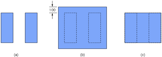 |
Hierarchical designs make life especially difficult for the CIF generator. The CIF corresponding to a collection of subcells may not necessarily be the same as the sum of the CIF's of the individual cells. For example, if a layer is generated by growing and then shrinking, nearby features from different cells may merge together so that they don't shrink back to their original shapes (see Figure 5). If Magic generates CIF separately for each cell, the interactions between cells will not be reflected properly. The CIF generator attempts to avoid these problems. Although it generates CIF in a hierarchical representation that matches the Magic cell structure, it tries to ensure that the resulting CIF patterns are exactly the same as if the entire Magic design had been flattened into a single cell and then CIF were generated from the flattened design. It does this by looking in each cell for places where subcells are close enough to interact with each other or with paint in the parent. Where this happens, Magic flattens the interaction area and generates CIF for it; then Magic flattens each of the subcells separately and generates CIF for them. Finally, it compares the CIF from the subcells with the CIF from the flattened parent. Where there is a difference, Magic outputs extra CIF in the parent to compensate.
Magic's hierarchical approach only works if the overall CIF for the parent ends up covering at least as much area as the CIFs for the individual components, so all compensation can be done by adding extra CIF to the parent. In mathematical terms, this requires each geometric operation to obey the rule
Op(AB)
Op(A)
The operations and, or, grow, and shrink all obey this rule. Unfortunately, the and-not, bloat, and squares operations do not. For example, if there are two partially-overlapping tiles in different cells, the squares generated from one of the cells may fall in the separations between squares in the other cell, resulting in much larger areas of material than expected. There are two ways around this problem. One way is to use the design rules to prohibit problem situations from arising. This applies mainly to the squares operator. Tiles from which squares are made should never be allowed to overlap other such tiles in different cells unless the overlap is exact, so each cell will generate squares in the same place. You can use the exact_overlap design rule for this.
The second approach is to leave things up to the designer. When generating CIF, Magic issues warnings where there is less material in the children than the parent. The designer can locate these problems and eliminate the interactions that cause the trouble. Warning: Magic does not check the squares operations for hierarchical consistency, so you absolutely must use exact_overlap design rule checks! Right now, the cifoutput section of the technology is one of the trickiest things in the whole file, particularly since errors here may not show up until your chip comes back and doesn't work. Be extremely careful when writing this part!
|
Another problem with hierarchical generation is that it can be very slow, especially when there are a number of rules in the cifoutput section with very large grow or shrink distances, such that magic must always expand its area of interest by this amount to be sure of capturing all possible layer interactions. When this "halo" distance becomes larger than the average subcell, much of the design may end up being processed multiple times. Noticeably slow output generation is usually indicative of this problem. It can be alleviated by keeping output rules simple. Note that basic AND and OR operations do not interact between subcells, so that rules made from only these operators will not be processed during subcell interaction generation. Remember that typically, subcell interaction paint will only be generated for layers that have a "grow" operation followed by a "shrink" operation. This common ruleset lets layers that are too closely spaced to be merged together, thus eliminating the need for a spacing rule between the layers. But consider carefully before implementing such a rule. Implementing a DRC spacing rule instead may eliminate a huge amount of output processing. Usually this situation crops up for auto-generated layers such as implants and wells, to prevent magic from auto-generating DRC spacing violations. But again, consider carefully whether it might be better to require the layout engineer to draw the layers instead of attempting to auto-generate them.
At the end of each style in the cifoutput section, one may include render statements, one per defined CIF/GDS layer. These render statements are used by the 3-D drawing window in the OpenGL graphics version of magic, and are also used by the "cif see" command to set the style painted. The syntax for the statement is as follows:
render cif_layer style_name height thickness
The cif_layer is any valid layer name defined in the same cifoutput section where the render statement occurs. The style_name is the name or number of a style in the styles file. The names are the same as used in the styles section of the technology file. height and thickness are effectively dimensionless units and are used for relative placement and scaling of the three-dimensional layout view (such views generally have a greatly expanded z-axis scaling). By default, all layers are given the same style and a zero height and thickness, so effectively nothing useful can be seen in the 3-D view without a complete set of render statements.
In addition to writing CIF, Magic can also read in CIF files using the cif read file command. The cifinput section of the technology file describes how to convert from CIF mask layers to Magic tile types. In addition, it provides information to the Calma reader to allow it to read in Calma GDS II Stream format files. The cifinput section is very similar to the cifoutput section. It can contain several styles, with a line of the form
style name
used to end the description of the previous style (if any), and start a new CIF input style called name. If no initial style name is given, the name default is assigned. Each style must have a statement of the form
scalefactor scale [nanometers]
to indicate the output scale relative to Magic units. Without the optional keyword nanometers, scale describes how many hundredths of a micron correspond to one unit in Magic. With nanometers declared, scale describes how many nanometers correspond to one unit in Magic.
Each style can specify several options affecting the behavior of the input. Currently, there are two options available. These may be specified one at a time, or all in the same statement, with options separated by space.
options ignore-unknown-layer-labels options no-reconnect-labels
The option "ignore-unknown-layer-labels" prevents magic from assigning layer types to labels in the input that do not correspond to a known layer type after processing. Such labels will be discarded. Otherwise, such labels will be attached (initially) to space and reconnected after processing.
The option "no-reconnect-labels" prevents magic from attempting to reassign label layers after processing. The input file does not require that a label correspond to any physical layer geometry in a cell (it may, for example, attach to layer geometry in a cell within the hierarchy of the cell the label is in). Note that only versions of magic since 8.0.139 will correctly extract a label that is not enclosed by paint of the same layer that the label is assigned to, or an electrically connected layer. Additionally, the enclosing layer must be in the same cell as the label.
Note also the use of the "text" keyword after the "labels" command (magic version 8.0 and above only), which can be used to prevent reconnecting labels for specific layers only.
Like the cifoutput section, each style consists of a number of layer descriptions. A layer description contains one or more lines describing a series of geometric operations to be performed on CIF layers. The result of all these operations is painted on a particular Magic layer just as if the user had painted that information by hand. A layer description begins with a statement of the form
layer magicLayer [layers]
In the layer statement, magicLayer is the Magic layer that will be painted after performing the geometric operations, and layers is an optional list of CIF layers. If layers is specified, it is the initial value for the layer being built up. If layers isn't specified, the layer starts off empty. As in the cifoutput section, each line after the layer statement gives a geometric operation that is applied to the previous contents of the layer being built in order to generate new contents for the layer. The result of the last geometric operation is painted into the Magic database.
The geometric operations that are allowed in the cifinput section are a subset of those permitted in the cifoutput section:
or layers
and layers
and-not layers
grow amount
shrink amount
In these commands the layers must all be CIF layers, and the amounts are all CIF distances (centimicrons, unless the keyword nanometers has been used in the scalefactor specification). As with the cifoutput section, layers can only be specified in simple comma-separated lists: tildes and slashes are not permitted.
When CIF files are read, all the mask information is read for a cell before performing any of the geometric processing. After the cell has been completely read in, the Magic layers are produced and painted in the order they appear in the technology file. In general, the order that the layers are processed is important since each layer will usually override the previous ones. For example, in the scmos tech file shown in Table 10 the commands for ndiff will result in the ndiff layer being generated not only where there is only ndiffusion but also where there are ntransistors and ndcontacts. The descriptions for ntransistor and ndcontact appear later in the section, so those layers will replace the ndiff material that was originally painted.
Labels are handled in the cifinput section just like in the cifoutput section. A line of the form
labels layers
means that the current Magic layer is to receive all CIF labels on layers. If the optional argument "text" is not specified (see below), then the layer type(s) in layers are only an initial layer assignment for the labels. Once a CIF or GDS cell has been read in, Magic scans the label list and re-assigns labels if necessary. In the example of Table 10, if a label is attached to the CIF layer CPG then it will be assigned to the Magic layer poly. However, the polysilicon may actually be part of a poly-metal contact, which is Magic layer pcontact. After all the mask information has been processed, Magic checks the material underneath the layer, and adjusts the label's layer to match that material (pcontact in this case). This is the same as what would happen if a designer painted poly over an area, attached a label to the material, then painted pcontact over the area.
Magic versions 8.0 and above allow additional options to the labels command:
labels layers [text | sticky]
labels layers port
labels layers cellid
The "text" option specifies that labels on this layer should be treated as comment or informational text only. Labels that meet this criterion may exist without attachment to physical layer geometry, and will never be reattached to another layer due to changes in the cell geometry. From magic version 8.0.139, labels assigned with the text option do not need to be restricted to informational text; they will be extracted correctly with respect to any electrically connected material in any overlapping cell. Also, from magic version 8.0.139, these so-called "sticky" labels retain their layer assignments when written to and read back from a magic database file.
"sticky" is an alias for "text", indicating that the labels must remain attached to the specified layer.
The "port" option specifies that labels on this layer are to be treated as ports of the cell. This option should be used when there is a specific layer name or GDS layer:purpose pair reserved for use as a "pin", not as plain text. Note that the GDS format is very limited in its ability to describe ports; port order cannot be encoded in GDS, so magic orders the ports in the order that they are found in the GDS stream.
The "cellid" option is a special option that specifies that a CIF/GDS text layer is used specifically to encode the name of the cell. This is used by some vendors to work around the 30-character limit of GDS cell names. The actual cell name is in the text string. The structure name in the input data is ignored, and replaced by the text string, renaming the cell. Typically, cellid will be mapped to a templayer, since there will not normally be a design layer associated with the cell identifier text.
Magic version 8.1 allows several additional options:
templayer layerName [layers]
This works in an analagous way to templayer in the cifoutput section; it defines a temporary CIF layer instead of a Magic layer type, and the CIF layer becomes the target of the boolean operations that follow the templayer statement. The layer layerName may be used subsequently in the cifinput section as if it were another input layer.
Magic version 8.1 up to revision 94 allowed this option:
fault layerName [layers]
Briefly, the purpose of fault was to identify a condition involving geometry that does not map to a magic database type, such as a bare contact cut with no layer context. Identifying non-mapping geometry would cause the entire cell geometry to be pulled up into the next level of cell hierarchy. Because this alters the hierarchy of the layout compared to the GDS or CIF file being read in, it was considered undesirable behavior, and was deprecated in magic version 8.1.94. From that version onward, "fault" is treated equivalently to "templayer", but is not backwards compatible. Instead, use the operator "copyup" described below.
copyup layers
Introduced in version 8.1.95, "copyup" is a geometry operator. Unlike other operators such as "and", "and-not", etc., there should only be one statement "copyup" per layer, and it may only be used for a templayer. The copyup operator may appear anywhere in the list, but the operation acts on the result of all other layer operators, so it is generally preferred to put it as the last operator for the layer.
Generally speaking, no hierarchical mask processing is done for CIF input. Each cell is read in and its layers are processed independently from all other cells; Magic assumes that there will not be any unpleasant interactions between cells as happens in CIF output. However, there are cases where this is not true, when reading GDS files that are created by tools other than Magic. Some tools will generate partial structures such as contact cuts without overlapping layers, or diffusion without implants, using them as simple cells that can be instanced and arrayed when needed. Partial structures like these are fundamentally incompatible with Magic's layer database. To avoid such problems, a templayer can be defined to identify geometry that does not map to a magic layer (such as a bare contact cut). At the end of the operations defining the templayer, the copyup operator tells the CIF or GDS read routine to save the geometry of the templayer locally in the cell. Whenever the cell is instantiated anywhere in the design, instead of instancing the cell, the saved geometry is "copied up" into the parent cell. If the parent cell contains the additional information needed to define a proper magic type (such as the layers on top and bottom of a bare contact cut), then the geometry will be resolved. If not, then the geometry will continue to be copied up the hierarchy until either it is resolved as a magic type, or the top level of the hierarchy is reached. If the geometry is unresolved by the top level cell, a warning is generated indicating that geometry in the input file has been lost.
The copyup function has one argument, which is a comma-separated list of one or more CIF/GDS layer types. When copying geometry up into the parent cell, the generated templayer geometry will be copied as many times as there are layers in the list, and each time assigned the indicated layer type. For example, a templayer called "barecontact" might be defined to identify bare contacts with no additional layers surrounding them. The resulting geometry would be copied up as the contact cut layer ("CONT", perhaps), and it might be preferred to also copy up the metal1 layer that is always present with such a contact.
Magic version 8.2.117 introduced this layer statement:
boundary
Magic version 8.3.117 introduced this layer statement:
not-square
Magic version 8.3.117 also allowed this operator in cifinput styles:
mask-hints layer_name
Magic version 8.3.619 introduced a way to handle input layers being tagged with text, which is common in some PDKs. This is equivalent to bloat-all except the starting point is the position of a label, rather than a layer. The syntax is:
tagged text [layers]
If Magic encounters a CIF layer name that doesn't appear in any of the lines for the current CIF input style, it issues a warning message and ignores the information associated with the layer. If you would like Magic to ignore certain layers without issuing any warning messages, insert a line of the form
ignore cifLayers
where cifLayers is a comma-separated list of one or more CIF layer names.
Calma layers are specified via calma lines, which should appear at the end of the cifinput section. They are of the form:
calma cifLayer calmaLayers calmaTypes
The cifLayer is one of the CIF types mentioned in the cifinput section. Both calmaLayers and calmaTypes are one or more comma-separated integers between 0 and 63. The interpretation of a calma line is that any Calma geometry whose layer is any of the layers in calmaLayers, and whose type is any of the types in calmaTypes, should be treated as the CIF layer cifLayer. Either or both of calmaLayers and calmaTypes may be the character * instead of a comma-separated list of integers; this character means all layers or types respectively. It is commonly used for calmaTypes to indicate that the Calma type of a piece of geometry should be ignored.
Just as for CIF, Magic also issues warnings if it encounters unknown Calma layers while reading Stream files. If there are layers that you'd like Magic to ignore without issuing warnings, assign them to a dummy CIF layer and ignore the CIF layer.
This section defines a mapping between magic layers and layers that may be found in LEF and DEF format files. Without the section, magic cannot read a LEF or DEF file. The LEF and DEF layer declarations are usually simple and straightforward (as they typically define metal layers only), so often it will suffice to insert a plain vanilla lef section into a technology file if one is missing. The lef section was introduced in technology file format 28, and is therefore absent from all .tech27 technology files. All of the statements in the lef section have the same format:
layer magic-type lefdef-type ...
cut magic-type lefdef-type ...
contact magic-type lefdef-type ...
route|routing magic-type lefdef-type ...
obstruction magic-type lefdef-type ...
obstruction magic-type1,magic-type2 lefdef-cut-type ...
masterslice magic-type lefdef-type ...
overlap magic-type lefdef-type ...
bound magic-type lefdef-type ...
ignore lefdef-type ...
Each statement defines a mapping between a Magic layer type magic-type and one or more type names lefdef-type (space-separated) that might be encountered in a LEF or DEF file. The different command names all refer to different type classes defined by the LEF/DEF specification. For most purposes, it is only necessary to use the layer statement. If the magic type is a contact type, then the layer statement is equivalent to specifying cut; otherwise, it is equivalent to route.
Because cut types in LEF files always describe the geometry of the contact cut itself, the section defines two separate statements for handling contacts. The "cut" statement should be used if the magic layer type magic-type corresponds to a layer representing a contact cut only. The "contact" statement has the same syntax as the "cut" statement but should be used if the magic layer type magic-type corresponds to a layer representing a contact area to be filled with cuts according to a generation rule in the cifoutput section, which is magic's normal way of handling contacts.
Note the special case of "obstruction" in which the magic tile type is a comma-separated list of exactly two types. Because magic contacts are normally defined as existing on the two metal planes they connect, rather than existing on a separate plane in-between, there may not be a correct way do define a via layer obstruction. In such a case, it may be helpful to define the LEF layer as corresponding to the two residue types that define the layers connected by the contact type.
The "bound" keyword indicates a Magic type that is a boundary (abutment) layer. Although LEF reads map a boundary layer to cell bounding boxes via a cell property, GDS has no such mapping and often encodes cell bounding boxes as a layer. If such a layer is mapped to a magic layer, then the lef section bound command maps this layer to the cell SIZE in the LEF macro definition.
The "ignore" keyword tells Magic to ignore the LEF layer types listed. Any geometry found defined on ignored layers will be discarded without comment. This can be useful, for example, to ignore geometry on the poly or active layers when one does not expect to route on the active plane.
Table 11 is a typical lef section for a 5-metal technology, which encompasses the most commonly used layer names found in LEF and DEF files.
|
This section defines the layers and contacts available to the Magic maze router, mzrouter, and assigns default costs for each type. Default widths and spacings are derived from the drc section of the technology file (described below) but can be overridden in this section. Other mzrouter parameters, for example, search rate and width, can also be specified in this section. The syntax and function of the lines in the mzrouter section of the technology file are specified in the subsections below. Each set of specifications should be headed by a style line. Routelayer and routecontact specifications should precede references to them.
The mzrouter is currently used in two contexts, interactively via the iroute command, and as a subroutine to the garouter (gate array router) for stem generation. To permit distinct parameters for these two uses, the lines in the mzrouter section are grouped into styles. The lines pertaining to the irouter should be preceded by
style irouter
and those pertaining to the garouter should be preceded by the specification
style garouter
Other styles can be specified, but are currently not used. Table 12 shows the mzrouter section from the scmos technology.
Layer lines define the route-layers available to the maze router in that style. They have the following form:
layer type hCost vCost jogCost hintCost
Here type is the name of the tiletype of the layer and hCost, vCost, jogCost and hintCost, are non-negative integers specifying the cost per unit horizontal distance, cost per unit vertical distance, cost per jog, and cost per unit area of deviation from magnets, respectively. Route layers for any given style must lie in distinct planes.
Versions of Magic beginning with 7.5.35 define the cost functions beyond the horizontal and vertical length costs as optional (defaulting to 1, the minimum cost), and add an additional cost value, the overCost. The overCost defines the cost of routing directly over an adjacent routing layer. A high value for overCost will tend to prevent the maze router from placing routes directly over other pins, thus preventing those pins from being routed. It will also tend to force the maze router to river route (route on a single layer) to a greater extent than otherwise, and avoid long paths with one signal directly on top of another, which exacerbates crosstalk problems. The layer syntax for magic 7.5.35 and higher is given below.
layer type hCost vCost [jogCost [hintCost [overCost]]]
Contact lines specify the route-contacts available to the mzrouter in the current style. They have the following form:
contact type routeLayer1 routeLayer2 cost
Here type is the tiletype of the contact, routeLayer1 and routeLayer2 are the two layers connected by the contact, and cost is a nonnegative integer specifying the cost per contact.
It may be desirable to have a layer or contact available to the maze router, but default to off, i.e., not be used by the mzrouter until explicitly made active. Route-types (route-layers or route-contacts) can be made to default to off with the following specification:
notactive route-type ...[route-typen]
The search rate, width, and penalty parameters can be set with a specification of the form:
search rate width penalty
Here rate and width are positive integers. And penalty is a positive rational (it may include a decimal point). See the irouter tutorial for a discussion of these parameters. (Note that penalty is a "wizardly" parameter, i.e., it is interactively set and examined via iroute wizard not iroute search). If no search line is given for a style, the overall mzrouter defaults are used.
Appropriate widths for route-types are normally derived from the drc section of the technology file. These can be overridden with width specifications of the following form:
width route-type width
Here width is a positive integer.
Minimum spacings between routing on a route-type and other types are derived from the design rules. These values can be overridden by explicit spacing specifications in the mzrouter section. Spacing specifications have the following form:
spacing routetype type1 spacing1 ...[typen spacingn]
Spacing values must be nonnegative integers or NIL. The special type SUBCELL can be used to specify minimum spacing to unexpanded subcells.
The design rules used by Magic's design rule checker come entirely from the technology file. We'll look first at two simple kinds of rules, width and and spacing. Most of the rules in the drc section are one or the other of these kinds of rules.
The technology file can contain several different specifications of DRC rules. Each of these is called a DRC style. Different styles may be used for fabrication at different feature sizes, or for other purposes. For example, some rules have a large "halo" (area of interaction surrounding an edge) that causes Magic's design rule checker to run very slowly, because it has to search large areas and often flatten large sections of hierarchical layout before it can perform each check. It is good practice to split the DRC deck into "quick and dirty" and "comprehensive" styles. The "quick and dirty" style will run interactively and catch most common design rule errors right away. The "comprehensive" style can be run occasionally to catch more obscure errors. Although Magic's design rule checker is very clever about checking only areas that have changed in a layout, certain actions, such as instancing a large subcell, or copying a large amount of paint, will require a complete set of checks. When these sort of actions cause Magic to run noticeably slower, it's time to consider splitting up the DRC deck.
The method of specifying styles in the drc section is very similar to the way it is done in the cifoutput and cifinput sections. The DRC deck can contain several styles, with a line of the form
style name
used to end the description of the previous style and start the description of a new style. The Magic command drc style name is typed by users to change the current style used for output. The first style in the technology file is used by default for DRC checking if the designer doesn't issue a drc style command. If the first line of the drc section isn't a style line, then Magic uses an initial style name of default.
Each style must contain a line of the form
scalefactor scale [reducer]
that tells how to scale DRC coordinates into Magic coordinates. The argument scale indicates how many DRC (distance) units correspond to one Magic unit. The argument reducer allows scalefactors to be represented as fractions represented by the integer ratio (scale / reducer). Note that both DRC units and magic's internal coordinate system are in dimensionless units. The scalefactor is designed to allow users to describe DRC distances in convenient values such as nanometers. However, it must be remembered that the DRC units are then only nanometers with respect to some output scale defined by the active cifoutput style. The most important property of the use of the DRC scale is that it allows DRC values to be specified in units that are finer than Magic's internal grid. Magic scales each DRC unit relative to it's internal scale, and if the internal scale is changed at any time, all DRC units are re-interpreted relative to the new scale. For example, if the scale value is 10, and the DRC deck declares the minimum width of metal1 paint to be 35, then the actual DRC distance of 3.5 internal units will be rounded up to 4. Therefore, a metal1 line 3 units wide is in error, but one 4 units wide is correct. If the internal database is then made finer by a factor of two using the "scalegrid 1 2" command, then the new DRC distance will be (3.5 * 2 =) 7 units, and is not rounded.
scale and the optional reducer must be integers. All distance units in the DRC deck also must be integers.
The minimum width of a collection of types, taken together, is expressed by a width rule. Such a rule has the form:
width type-list width error
where type-list is a set of tile types (see Section 8 for syntax), width is an integer, and error is a string, enclosed in double quotes, that can be printed by the command drc why if the rule is violated. A width rule requires that all regions containing any types in the set types must be wider than w in both dimensions. For example, in Table 14, the rule
width nwell 6 "N-Well width must be at least 6 (MOSIS rule #1.1)"
means that nwells must be at least 6 units wide whenever they appear. The type-list field may contain more than a single type, as in the following rule:
width allDiff 2 "Diffusion width must be at least 2 (MOSIS rule #2.1)"
which means that all regions consisting of the types containing any kind of diffusion be at least 2 units wide. Because many of the rules in the drc section refer to the same sets of layers, the #define facility of the C preprocessor is used to define a number of macros for these sets of layers. Table 13 gives a complete list.
All of the layers named in any one width rule must lie on the same plane. However, if some of the layers are contacts, Magic will substitute a different contact image if the named image isn't on the same plane as the other layers.
There is an option available for a more obscure rule that requires that a certain layer type must be wider when that type is drawn at an angle than when it is drawn straight. The option is:
width type-list width angles error
The second simple kind of design rule is a spacing rule. It comes in four flavors: touching_ok, touching_illegal, surround_ok, manhattan_dist, and corner_ok. The first four adjacency flavors use the following syntax:
spacing types1 types2 distance adjacency error
The first adjacency class, touching_ok, does not prohibit types1 and types2 from being immediately adjacent. It merely requires that any type in the set types1 must be separated by a "Manhattan" distance of at least distance units from any type in the set types2 that is not immediately adjacent to the first type. See Figure 16.2 for an illustration of Manhattan distance for design rules. (Note that Euclidean distance measurements for design rules can be enabled using the command "drc euclidean on".) As an example, consider the polysilicon separation rule:
spacing allPoly allPoly 2 touching_ok \
"Polysilicon spacing must be at least 2 (MOSIS rule #3.2)"
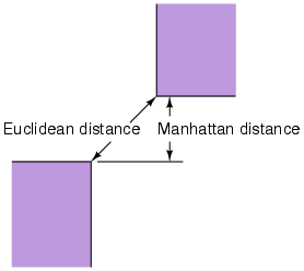 |
This rule is symmetric (types1 is equal to types2), and requires, for example, that a pcontact be separated by at least 2 units from a piece of polysilicon. However, this rule does not prevent the pcontact from touching a piece of poly. In touching_ok rules, all of the layers in both types1 and types2 must be stored on the same plane (Magic will substitute different contact images if necessary).
| ||||||||||||||||||||||||||||||
TOUCHING_OK SPACING RULES DO NOT WORK FOR VERY LARGE SPACINGS (RELATIVE TO THE TYPES INVOLVED). See Figure 6 for an explanation. If the spacing to be checked is greater than the width of one of the types involved plus either its self-spacing or spacing to a second involved type, touching_ok spacing may not work properly: a violation can be masked by an intervening touching type. In such cases the rule should be written using the edge4way construct described below.
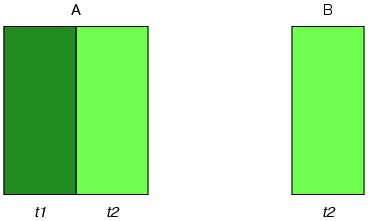 |
The second class of spacing rule, touching_illegal, disallows adjacency. It is used for rules where types1 and types2 can never touch, as in the following:
spacing pc allDiff 1 touching_illegal \
"Poly contact must be 1 unit from diffusion (MOSIS rule #5B.6)"
Pcontacts and any type of diffusion must be at least 1 unit apart; they cannot touch. In touching_illegal rules types1 and types2 may not have any types in common: it would be rather strange not to permit a type to touch itself. In touching_illegal rules, types1 and types2 may be spread across multiple planes; Magic will find violations between material on different planes.
The third class of spacing rule, surround_ok, was introduced in Magic version 7.5.24. It effectively removes the restriction that touching_ok cannot be used when the two types in the spacing rule are in different planes. This rule is implemented such that the material of types2 must completely surround the material of types1. (it may be necessary to implement a separate "coincidence_ok" rule, but this has not been done). The usual application of this rule is to implement, for example, distance from diffusion in nwell to a (different) nwell edge. Another useful application is to check the distance from a capacitor bottom plate to the edge of another piece of metal (or polysilicon) that is the same type as is used for the capacitor bottom plate.
The fourth class of spacing rule, manhattan_dist, forces the corner areas of the rule to be checked per manhattan distance rules, not euclidean distance rules. This is needed for certain situations where distance is checked to a CIF layer that is not visible but which can be inferred as extending from a junction of two layers. The most common use case is an implant layer such as P+ or N+ which ends at a butting junction. The measured distance would be to the corner of the butting material, but since the implant extends outward from the junction, the entire corner area must be checked for a spacing violation.
If euclidean checks are not enabled, then this rule is the same as the touching_illegal rule.
Finally, the fifth class of spacing rule, corner_ok, was introduced in Magic version 7.5.52, and has a slightly different syntax:
spacing types1 types2 distance corner_ok types3 errorIn this instance, we want to set the minimum allowed spacing between types types1 and types2. However, these types may be allowed to intersect when forming a device (if they did not form a specific device, then a crossing or intersection would be a violation), such as a transistor or capacitor. A typical example would be:
spacing allPolynotFET allActivenotFET 1 corner_ok allFETs \This example indicates that poly and diffusion cannot touch, but they are allowed to intersect where they form a transistor.
"Poly must be 1 unit from diffusion"
Many fabrications processes require a larger distance between layers when the width and length of one of those layers exceeds a certain minimum dimension. For instance, a process might declare that the normal spacing between metal1 lines is 3 microns. However, if a metal1 line exceeds a width of 100 microns, then the spacing to other unrelated metal1 lines must increase to 10 microns. This situation is covered by the widespacing rule. The syntax for widespacing is as follows:
widespacing types1 wwidth types2 distance flavor error
The widespacing rule matches the syntax of spacing in all respects except for the addition of the parameter wwidth, which declares the minimum width of layers of type(s) types1 that triggers the rule. So for the example above, the correct widespacing rule would be (assuming 1 magic unit = 1 micron):
widespacing allMetal1 100 allMetal1 10 touching_ok \
"Space to wide Metal1 (length and width 100) must be at least 10"
widespacing types1 wwidth runlength types2 distance flavor error
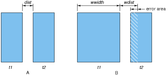 |
The surround rule specifies what distance a layer must surround another, and whether the presence of the surrounding material is optional or mandatory. This rule is designed for materials which must completely surround another, such as metal around a contact cut or MiM capacitor layer. The syntax is:
surround types1 types2 distance [distance2] presence error
and states that the layers in types2 must surround the layers in types1 by an amount distance lambda units. The value of presence must be one of the keywords absence_ok, absence_illegal, or (see below) directional. When presence is absence_illegal, then types types2 must always be present when types types1 are present. When presence is absence_ok, types types1 may exist outside of types types2 without error, but where they coincide, types types2 must overlap types1 by the amount distance.
The presence keyword "directional", added to Magic version 8.0.175 (July 2014), adds the capability to handle situations where a material is allowed to have a smaller amount of overlap on sides of an adjoining material (usually a contact cut) if the material overlaps by a larger amount on the orthogonal sides. Typically, this rule is applied to contact cuts on processes with feature sizes of 180nm or smaller, where such rules are common. Standard cell routing is facilitated by the smaller surround requirement, which allows the standard cell routing pitch to be smaller. The extra overlap length on the orthogonal sides of the contact cut increases the reliability of the contact and improve process yield.
The "directional" rule type was extended (Nov 2022) to include a second distance (distance2) for rules of the type "if metal overlaps via by less than distance2 on one side, then metal must overlap by at least distance on the adjacent side".
Note that the "directional" rule variation, as written, specifies only the larger of the two overlap distances. The lesser of the two overlap distances is assumed to be zero. Typically, a magic techfile will declare a contact type to include the dimensions of the smallest surrounding material requirement, in which case the smaller of the two overlap distances is, by definition, zero. However, if the techfile is defined differently, such as with contact cuts being drawn explicitly, and the smaller overlap distance is non-zero, then the smaller overlap distance requirement can be covered by an additional surround rule with "absence_illegal".
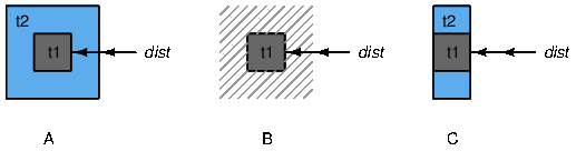 |
overhang types1 types2 distance error
and states that layers in types1 must overhang layers in types2 by an amount distance lambda units. The rule flags the complete absence of types types1, but does not prohibit the use of types1 as a bridge (that is, with types types2 on either side of types1, which will generally be covered by a separate spacing rule, and which may have a different spacing requirement).
The Extend rule is very similar to the Overhang rule. The primary difference is that "Overhang" assumes that the layers in types2 must always be present, and that it is an error for them to be missing. The extend rule covers cases in which a layer must be a certain length when it is present, but it is not an error for it to be absent. The most typical application is to specify a minimum length for a device such as a transistor or resistor. The syntax is exactly like overhang:
extend types1 types2 distance errorAnd states that layers in types1, where they abut layers in types2, must extend outward from types2 by an amount distance. It is not necessary for types1 and types2 to be in the same plane. An example of the typical use to declare a minimum transistor length is:
extend nfet *ndiff 3 \There are two options available with the extend rule, which are:
"N transistor length must be at least 3"
extend types1 types2 distance exact_width errorand
extend types1 types2 distance exclusive errorThe exact_width option, as the name implies, indicates that types1 must extend from types2 to a distance of exactly distance, neither more nor less. This is useful for implementing rules for devices which have fixed layout dimensions.
The exclusive option indicates that layers2 may not appear within distance of the edge between layers2 and layers1. This distinguishes between two types of extension: For example, minimum extension of diffusion from a transistor gate would include any additional gates found within the measured distance, since those gates also have diffusion underneath. But extension of a gate from diffusion implies that the extend rule is being used to specify a minimum length of a gate, for which the gate type is the only type that may be found for length distance from the edge. This use of extend requires the exclusive option.
The rect_only rule is used to denote layers that must be rectangular; that is, they cannot bend, or have notches or tabs. Generally, this is used for contacts, so that the CIF output operator squares will be guaranteed to generate a correct contact. This is due to magic's corner-stitching tile database, where bends, notches, tabs, and slots will break up an otherwise continuous patch of material into potentially many small tiles, each one of which might be too small to fit a contact cut.
rect_only types error
angles types allowed why
The width and spacing rules just described are actually translated by Magic into an underlying, edge-based rule format. This underlying format can handle rules more general than simple widths and spacings, and is accessible to the writer of a technology file via edge rules. These rules are applied at boundaries between material of two different types, in any of four directions as shown in Figure 10. The design rule table contains a separate list of rules for each possible combination of materials on the two sides of an edge.
 |
In its simplest form, a rule specifies a distance and a set of mask types: only the given types are permitted within that distance on type2's side of the edge. This area is referred to as the constraint region. Unfortunately, this simple scheme will miss errors in corner regions, such as the case shown in Figure 11. To eliminate these problems, the full rule format allows the constraint region to be extended past the ends of the edge under some circumstances. See Figure 12 for an illustration of the corner rules and how they work. Table 16 gives a complete description of the information in each design rule.
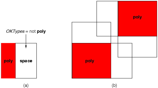 |
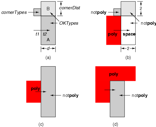 |
|
Edge rules are specified in the technology file using the following syntax:
edge types1 types2 d OKTypes cornerTypes cornerDist error [plane]
Both types1 and types2 are type-lists. An edge rule is generated for each pair consisting of a type from types1 and a type from types2. All the types in types1, types2, and cornerTypes must lie on a single plane. See Figure 12 for an example edge rule. It is sometimes useful to specify a null list, i.e., 0, for OKTypes or CornerTypes. Null OKTypes means no edges between types1 and types2 are OK. Null CornerTypes means no corner extensions are to be checked (corner extensions are explained below).
Some of the edge rules in Magic have the property that if a rule is violated between two pieces of geometry, the violation can be discovered looking from either piece of geometry toward the other. To capitalize on this, Magic normally applies an edge rule only in two of the four possible directions: bottom-to-top and left-to-right, reducing the work it has to do by a factor of two. Also, the corner extension is only performed to one side of the edge: to the top for a left-to-right rule, and to the left for a bottom-to-top rule. All of the width and spacing rules translate neatly into edge rules.
However, you'll probably find it easiest when you're writing edge rules to insist that they be checked in all directions. To do this, write the rule the same way except use the keyword edge4way instead of edge:
edge4way nfet ndiff 2 ndiff,ndc ndiff 2 \
"Diffusion must overhang transistor by at least 2"
Not only are edge4way rules checked in all four directions, but the corner extension is performed on both sides of the edge. For example, when checking a rule from left-to-right, the corner extension is performed both to the top and to the bottom. Edge4way rules take twice as much time to check as edge rules, so it's to your advantage to use edge rules wherever you can.
| ||||||||||||||||||||||||||||||||||||||||||
Normally, an edge rule is checked completely within a single plane: both the edge that triggers the rule and the constraint area to check fall in the same plane. However, the plane argument can be specified in an edge rule to force Magic to perform the constraint check on a plane different from the one containing the triggering edge. In this case, OKTypes must all be tile types in plane. This feature is used, for example, to ensure that polysilicon and diffusion edges don't lie underneath metal2 contacts:
edge4way allPoly ~(allPoly)/active 1 ~m2c/metal2 ~(allPoly)/active 1 \
"Via must be on a flat surface (MOSIS rule #8.4,5)" metal2
Magic versions using techfile formats more recent than 28 are generally more clever about determining the correct plane from OKTypes when they differ from the triggering types, and the situation is unambiguous (use of "space" in rules tends to introduce ambiguity, since space tiles appear on all planes).
In order for CIF generation and circuit extraction to work properly, certain kinds of overlaps between subcells must be prohibited. The design-rule checker provides two kinds of rules for restricting overlaps. They are
exact_overlap type-list
no_overlap type-list1 type-list2
In the exact_overlap rule, type-list indicates one or more tile types. If a cell contains a tile of one of these types and that tile is overlapped by another tile of the same type from a different cell, then the overlap must be exact: the tile in each cell must cover exactly the same area. Abutment between tiles from different cells is considered to be a partial overlap, so it is prohibited too. This rule is used to ensure that the CIF squares operator will work correctly, as described in Section 12.6. See Table 18 for the exact_overlap rule from the standard scmos technology file.
The no_overlap rule makes illegal any overlap between a tile in type-list1 and a tile in type-list2. You should rarely, if ever, need to specify no_overlap rules, since Magic automatically prohibits many kinds of overlaps between subcells. After reading the technology file, Magic examines the paint table and applies the following rule: if two tile types A and B are such that the result of painting A over B is neither A nor B, or the result of painting B over A isn't the same as the result of painting A over B, then A and B are not allowed to overlap. Such overlaps are prohibited because they change the structure of the circuit. Overlaps are supposed only to connect things without making structural changes. Thus, for example, poly can overlap pcontact without violating the above rules, but poly may not overlap diffusion because the result is efet, which is neither poly nor diffusion. The only no_overlap rules you should need to specify are rules to keep transistors from overlapping other transistors of the same type.
The off_grid rule is, like the no_overlap rule, generally not needed. Magic generally has a base internal database unit that equals the minimum manufacturing grid. If the cifoutput section of the techfile declares a grid limit, then making the internal grid smaller than this value is prohibited. Then it becomes impossible to specify off-grid geometry except in one specific case mentioned below. However, it is possible to set up the tech file without a grid limit, and read in arbitrary GDS which may or may not align to the manufacturing grid, in which case the off_grid rule can detect and flag such errors. The syntax is:
off_grid types pitch why
Types is a list of types that will be checked for off-grid positions, and may be any set of types with no restrictions. Pitch is the spacing of the mininum manufacturing grid.
As mentioned above, there is one instance in which off-grid positions can be created, and that is the case of having non-Manhattan geometry in two different cells, overlapping. It is possible for two non-Manhattan shapes to have all vertices on the manufacturing grid, but their point of intersection is off-grid. Since this condition can be detected when flattening the layout for hierarchical DRC checks, the off-grid intersection is flagged by the DRC engine independently of any rule.
The area rule is used to check the minimum area of a region. Its syntax is:
area types minarea minedge why
Types is a list of types that compose the region, all of which must be on the same plane. Minarea is the minimum area that a region must have, while minedge is the minimum length of an edge for the region. This second dimension is basically an optimization to make the design rule checker run faster; without it, the checker has to assume that a region 1 lambda wide and minarea long is legal, and it must examine a much larger area when checking the interaction between cells. Specifying minedge reduces this interaction distance. An example rule is:
area (emitter,em1c)/npoly 6 2 "emitter must be at least 2x3"
Another use for the area rule is to force a minimum metal extension on contacts. Many processes allow contact cuts to be surrounded by a minimum (even zero) amount of metal, provided that extra surrounding metal is provided on either side of the contact in the other direction. One way to implement this type of rule is to write the cifoutput rules to generate the minimum metal surround, but use the minimum area rule to insist that contact cuts must be wide enough at minimum height to provide the necessary extra metal extension on each side of the cut. In that case, the minedge distance should be the length of the cut plus metal extension in both directions.
Sometimes a technology requires that a region not be wider than a certain value. The maxwidth rule can be used to check this.
maxwidth layers mwidth [bends] [exclude_layers] why
Layers, the types that compose the region, must all be in the same plane. The region must be less than mwidth wide in either the horizontal or vertical dimension. Bends takes one of three values, bend_illegal, bend_ok, or both. For bend_illegal rules, the checker forms a bounding box around all contiguous tiles of the correct type, then checks this box's width. For example:
maxwidth (emitter,em1c)/npoly 2 bend_illegal \
"emitter width cannot be over 2"
bend_ok rules are used to check structures where the region must be locally less than maxwidth, but may contain bends, T's, and X's. If bends is not present, then bend_ok is assumed.
For bend_ok and bend_illegal, the width must be violated in both directions. The option both instead checks that either dimension exceeds the maximum width.
maxwidth trench 2 bend_ok "trench must be exactly 2 wide"
The bend_ok rule uses a completely different algorithm than the bend_illegal case. The bounding box is made in a similar fashion to that described for bend_illegal. Then types inside the bounding box that are not of types in layers cause the bounding box to be clipped, and possibly divided into several areas, each representing a possible maximum-size rectangle. Any rectangle is found that is larger than the mwidth after all clipping has taken place is a DRC violation.
Warning: The bend_ok rule only searches for Manhattan maximum-size rectangles. It is possible to create areas which exceed the maximum width in a non-Manhattan direction but which pass Magic's maxwidth rule.
Figure 14 shows some examples of both types of rules.
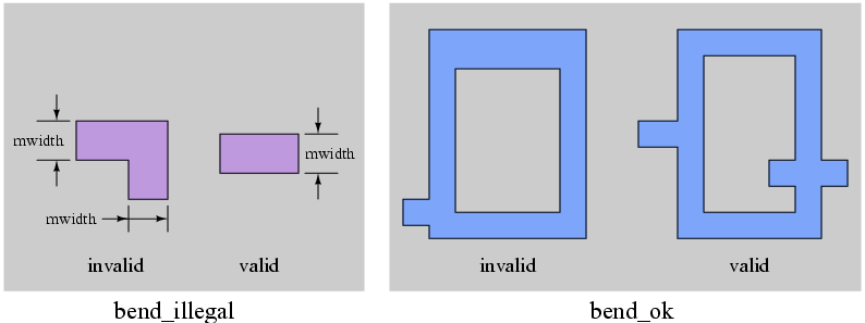 |
From magic version 8.3.571, an additional set of layers exclude_layers may be specified. The layers in exclude_layers must all lie in the same plane, if more than one layer is specified, and may not be in the same plane as the type being checked for maxwidth. The layers comprise a set which, if overlapping layers, will prevent the maxwidth rule from being applied. A typical use case for this is when a top metal layer larger than some value must be slotted, but that rule is excepted for pads. The passivation cut layer can then be used to exclude the pad from maxwidth checks.
In magic version 8.3.616, the concept of sets of rule exceptions and exemptions was introduced. Some DRC rule specifications will present a DRC rule, and then give a list of exceptions to that rule in certain contexts which are usually determined by the presence of a marker ID layer. The exemptions are usually less strict than the regular rule, but can be stricter, or possibly the rule does not apply at all (is "exempted") in a given context.
For example, a common usage is to have certain relaxed rules for SRAM layouts. The relaxed rules allow the SRAM core cell to be compressed to a size smaller than could be achieved with the standard DRC rules. The compressed rules are allowable only because the SRAM core layout is highly regular and arrayed. Such relaxed rules would not be allowable outside of the context of an SRAM core bit array.
Prior to magic version 8.3.616 (implemented in March 2026), the only way to handle a rule exemption was to create an additional layer for the exceptional context, and to apply a different set of rules for that special layer. That method works, but it has the drawback of making the tech file messy and adding a potentially large number of extra, special-purpose layers. It greatly increases the size and complexity of the tech file, and raises the risk of errors in the tech file.
The newer method introduces two new statements to the tech file drc section, the "exception" statement and the "exemption" statement:
exception name|none
exemption name|none
Each of these statements takes exactly one argument, either a name which is an arbitrary string, or the keyword none, which ends the rule exception or exemption group. name is the name of a marker layer in the form of a "mask-hint" property (see the cifinput section for an explanation of mask-hints). The mask-hint layer can be manually generated using the property command, but more typically, it will be generated automatically from GDS input data using a mask-hint rule in the cifinput section. In both sections, name is the simple name of the mask ID layer (e.g., "SRAMID"), while the property itself has a key name with "MASKHINTS_" prefixed to the name (e.g., property key "MASKHINTS_SRAMID"). A mask-hint property value always consists of sets of four coordinates marking the corners of bounding boxes for the layer. Whenever a rule check edge occurs inside one of those areas, the rule exception or exemption applies. For a rule exception, if the rule check edge is inside the mask-hint area specified by name, then the rule is applied to that edge, and otherwise the rule is skipped. For a rule exemption, if the rule check edge is inside the mask-hint area specified by name, then the rule is skipped; otherwise it is applied to that edge. Note that rule exceptions and exemptions only apply to edge-based rules, and will not affect the CIF rules (e.g., cifmaxwidth). Since CIF rules have direct access to mask layers, the behavior with respect to specific mask layers can be encoded directly into the CIF rules.
Both exception and exemption statements modify the same setting, so exception none and exemption none are equivalent statements.
Note that checking all layout for the presence or absence of a layer can be compute-intensive. The use of both exception and exemption is intended to reduce that overhead. If a rule is neither an exception nor an exemption, then there is no overhead whatsoever. If a rule is an exception or an exemption but no mask-hint area name is defined in the cell, then the only overhead is a property name look-up.
Starting in magic version 8.2.88, magic allows the distance value in a "why" string to be replaced by an escape code similar to C printf syntax. When printing a DRC error reason, the escape string is substituted with the actual physical distance value in microns as interpreted by the current value of the output scaling (per the CIF output style), and the current scalefactor. This way, the reported DRC dimensions scale with the choice of output scale, and (more subtlely) with the grid size. The grid size scaling causes values to be rounded to the nearest internal unit. Thus if internal units are in lambda units, the reported value is rounded to the nearest lambda.
The escape value "%d" is replaced with the normal distance value of the rule (e.g., width for width rules, spacing for spacing rules).
The escape value "%c" is replaced with the corner distance value of the rule.
The escape value "%a" is replaced with the area value of the rule (and with appropriate units), for area rules only.
For technologies with complicated generated layers, it is often difficult to check design rules on the abstract types that are drawn in Magic. To ameliorate this problem, the extended checker allows simple checks to be performed on cif layers. The rules that can be checked are width, spacing, area, and maxarea. Since checking rules on the CIF layers requires that these layers be generated, these checks are considerably slower than the normal ones, and should only be used when absolutely necessary.
The cifstyle rule is used to select which cifoutput style is used.
cifstyle cif_style
Cif_style must be one of the cif styles included in the cifoutput section. In the current implementation, the cif checker generates all the layers in the style regardless of whether they are actually used in design-rule checks; for speed, defining a separate cif style for design rule checking it may be worthwhile when only a few layers are checked. Any layer in the cif style, defined by either a layer or a templayer rule, may be checked.
The syntax for cifwidth is analogous to that of the regular width rule:
cifwidth layer width why
Layer is a single cif layer. (To do width checks with more than one cif layer, or all the layers into a new templayer). Width is the minimum width of the region in centimicrons.
The cifspacing rule is also very similar to the regular rule:
cifspacing layer1 layer2 separation adjacency why
Layer1 and layer2 are both cif layers. If adjacency is touching_ok, then layer1 must equal layer2. For touching_illegal rules, layer1 and layer2 may be any two cif layers. Separation is given in centimicrons.
The CIF area rule is:
cifarea layer minarea minedge why
Layer is again a single cif layer. minedge is expressed in centimicrons, and minarea is given in square centimicrons.
The CIF maxwidth rule is:
cifmaxwidth layer mwidth [bends] why
Again, layer is a single cif layer, and mwidth is given in centimicrons. bends may be one of "bend_ok", "bend_illegal", or "both". If left out, "bend_ok" is assumed. The interpretation of bends is the same as for the maxwidth rule.
Note that cifmaxwidth with mwidth = 0 will produce errors on any CIF layer paint remaining after a set of boolean operations. This is a good way to produce results on a number of types of DRC rules that cannot be done with edge-based rules, and closely matches the method of generating DRC errors used by Calibre. When mwidth is zero, "bends" is irrelevant, and should be left out. Magic will choose the fastest algorithm to run in this case.
Magic's background design-rule checker breaks large cells up into smaller pieces, checking each piece independently. For very large designs, the number of pieces can get to be enormous. If designs are large but sparse, the performance of the design-rule checker can be improved tremendously by telling it to use a larger step size for breaking up cells. This is done as follows:
stepsize stepsize
which causes each cell to be processed in square pieces of at most stepsize by stepsize units. It is generally a good idea to pick a large stepsize, but one that is small enough so each piece will contain no more than 100 to 1000 rectangles.
Note that the distances declared in the DRC section are used to determine the "halo" of possible interactions around a tile edge. Magic must consider all paint in all cells simultaneously; thus for each edge in the design, magic must flatten the hierarchy around it to a distance equal to the interaction halo. Clearly this has a huge impact on processing time. Because the DRC is interactive, the performance hit can be noticeable to downright irritating. Often this performance hit can be greatly reduced by removing rules with large distance measures, such as rules involving distances to pads, and widespacing rules. If this is a problem, consider using one technology file for layout, and one which can be used "offline" to do a slow, non-interactive DRC check for pad and widespacing rules on an entire project layout.
option option_name
Currently only one option is supported, option_name = wide-width-inclusive. When wide-width-inclusive is declared, all widespacing rules are interpreted as being triggered by material larger than or equal to the given material width. The default behavior is to interpret such rules as being triggered by material that is strictly larger than the given material width.
The extract section of a technology file contains the parameters used by Magic's circuit extractor. Each line in this section begins with a keyword that determines the interpretation of the remainder of the line. Table 19 gives an example extract section.
|
This section is like the cifinput and cifoutput sections in that it supports multiple extraction styles. Each style is preceded by a line of the form
style stylename
All subsequent lines up to the next style line or the end of the section are interpreted as belonging to extraction style stylename. If there is no initial style line, the first style will be named "default".
The statement units microns declares that all values in the extract section that are related to length will be given in units of microns, while values related to area will be given in units of microns squared. The alternative declaration is units lambda, which is the default if the "units" statement is not used, and declares that all values related to length will be given in units of lambda, while values related to area will be given in units of lambda squared. Values affected are those given in any statement in the extract section for area capacitance, perimeter and overlap capacitances, coupling capacitance, side halo, and step size.
The substrate statement is available from Magic version 8.1. It takes the following syntax:
substrate types plane [subs-name] [-id_types]
Magic version 8.2.141 introduced the additional option "-id_types", where id_types is a comma-separated list of types that are considered to shield layers above from the substrate; that is, if any type in types that is coincident with any type in id_types is not part of the substrate. This is useful in several ways; one, to declare a separate plane for a deep well, such that types like P+ diffusion can keep the same usage inside a deep N-well structure, but the P-well underneath the diffusion is not connected to the substrate because it is shielded by the deep N-well. Two, one can declare a special layer that blocks the extraction of substrate under it.
Note that it is not always best to define the lowest plane as substrate, although that would seem to be the most obvious choice. In the deep N-well example above, the deep N-well is the lowest plane, but it is more convenient to locate substrate on the well plane above it. That way, the use of space/w (space on the well plane) to indicate substrate works for devices outside deep N-well, and since the deep N-well is a shield type, nothing inside a deep N-well will be considered part of the substrate.
Magic version 8.3.20 introduced the optional argument subs-name, indicating a global name to use for the substrate (if unconnected to anything giving it a name with a higher priority, such as a labeled node). The intended use is with a Tcl variable name, e.g., "$SUB", which can then be set on a per-design basis. Use the name with caution, since if not used with a variable name, it sets a hard-coded name that might collide with another name in a design. If not specified, then the substrate node name will be the default automatically-generated node name. If the substrate includes "space/w" (as explained above), then the default name is "w_n1073741817_n1073741817# (indicating a position on the well plane at the most negative coordinate possible).
The keywords areacap, perimcap, and resist define the capacitance to substrate and the sheet resistivity of each of the Magic layers in a layout. All capacitances that appear in the extract section are specified as an integral number of attofarads (per unit area or perimeter), and all resistances as an integral number of milliohms per square.
The areacap keyword is followed by a list of types and a capacitance to substrate, as follows:
areacap types C
Each of the types listed in types has a capacitance to substrate of C attofarads per square lambda. Each type can appear in at most one areacap line. If a type does not appear in any areacap line, it is considered to have zero capacitance to substrate per unit area. Since most analysis tools compute transistor gate capacitance directly from the area of the transistor's gate, Magic should produce node capacitances that do not include gate capacitances. To ensure this, all transistors should have zero areacap values.
The perimcap keyword is followed by two type-lists and a capacitance to substrate, as follows:
perimcap intypes outtypes C
Each edge that has one of the types in intypes on its inside, and one of the types in outtypes on its outside, has a capacitance to substrate of C attofarads per lambda. This can also be used as an approximation of the effects due to the sidewalls of diffused areas. As for areacap, each unique combination of an intype and an outtype may appear at most once in a perimcap line. Also as for areacap, if a combination of intype and outtype does not appear in any perimcap line, its perimeter capacitance per unit length is zero.
The resist keyword is followed by a type-list and a resistance as follows:
resist types R [chop]
The sheet resistivity of each of the types in types is R milliohms per square. The optional value "chop" indicates the factor to apply to corners for the adjustment of resistance where devices bend at a 90 degree angle. The resistance through the corner as computed by the material resistance in ohms per square multiplied by the length of the path centerline will be multiplied by chop. The default value of chop if unspecified is 1.0. Typical values are 0.7 (the length difference of drawing the centerline across the corner at a 45 degree angle) or 0.5 (a more comprehensive number taking into account the increased effective width of material at the corner). While the chop value affects resistance calculations, it does so by modifying the effective width of the material at the corner; therefore, it also affects the calculation of device widths, such as that of transistors having gates with 90 degree bends.
Each resist line in fact defines a "resistance class". When the extractor outputs the area and perimeter of nodes in the .ext file, it does so for each resistance class. Normally, each resistance class consists of all types with the same resistance. However, if you wish to obtain the perimeter and area of each type separately in the .ext file, you should make each into its own resistance class by using a separate resist line for each type.
Starting in magic version 8.1.91, the value R may be specified as "None", in which case the types in the list types will not be considered for extraction of nodes. Non-mask types such as boundary or marker types should be handled this was, as should implant types like silicide block (where, for example, silicide block creates a resistor, the resistor has its own type; the silicide block layer itself is not functionally meaningful to magic). Otherwise, such layers will be extracted as nodes, may end up as ports to subcells, and create problems with LVS (layout vs. schematic) comparison tools.
In addition to sheet resistivities, there are two other ways of specifying resistances. Neither is used by the normal Magic extractor, but both are used by the resistance extractor. Contacts have a resistance that is inversely proportional to the number of via holes in the contact, which is proportional (albeit with quantization) to the area of the contact. The contact keyword allows the resistance for a single via hole to be specified:
contact types size R
contact types size border separation R
where types is a comma-separated list of types, size is in lambda, and R is in milliohms. Size is interpreted as a hole-size quantum; the number of holes in a contact is equal to its width divided by size times its length divided by size, with both quotients rounded down to the nearest integer. The resistance of a contact is R divided by the number of holes. The size alone may not compute the same number of contact cuts as would be generated by the cifoutput command, since it has no understaning of border and separation, and therefore may compute an incorrect contact resistance. To avoid this problem, the second form provides a way to give values for border and separation, again in units of lambda. There is no automatic check to guarantee that the extract and cifoutput sections agree on the number of contact cuts for a given contact area.
In magic versions 7.4 and 7.5, the contact statement is ignored. Contact cut rules are determined from the cifoutput rule decks, using exact values of border, size, and separation from "squares" and similar rules.
Transistors also have resistance information associated with them. However, a transistor's resistance may vary depending on a number of variables, so a single parameter is generally insufficient to describe it. The fetresist line allows sheet resistivities to be given for a variety of different configurations:
fetresist fettypes region R
where fettypes is a comma-separated list of transistor types (as defined in fet lines below), region is a string used to distinguish between resistance values for a fet if more than one is provided (the special region value of "linear" is required for the resistance extractor), and R is the on-resistance of the transistor in ohms per square (not milliohms; there would otherwise be too many zeroes).
devresist devicetypes resisttype R
The devresist is similar to fetresist but applies to device types other than MOSFETs. It allows for extraction of resistance that is not sheet resistance (which would be specified by the resist statement). The resisstype is a keyword which is specific to the type of device. Supported types are "area" and "perimeter" to support a vertical resistance between two planes. This could be used, for example, to extract a resistance through a tap or a diode series resistance. It is used in conjunction with a parameter type "r" and is automatically assumed for devices in which terminals exist on a different plane than the device.
Magic also extracts internodal coupling capacitances, as illustrated in Figure 13. The keywords overlap, sidewall, sideoverlap, and sidehalo provide the parameters needed to do this.
Overlap capacitance is between pairs of tile types, and is described by the overlap keyword as follows:
overlap toptypes bottomtypes cap [shieldtypes]
where toptypes, bottomtypes, and optionally shieldtypes are type-lists and cap is a capacitance in attofarads per square lambda. The extractor searches for tiles whose types are in toptypes that overlap tiles whose types are in bottomtypes, and that belong to different electrical nodes. (The planes of toptypes and bottomtypes must be disjoint). When such an overlap is found, the capacitance to substrate of the node of the tile in toptypes is deducted for the area of the overlap, and replaced by a capacitance to the node of the tile in bottomtypes.
 |
If shieldtypes are specified, overlaps between toptypes and bottomtypes that also overlap a type in shieldtypes are not counted. The types in shieldtypes must appear on a different plane (or planes) than any of the types in toptypes or bottomtypes.
 |
Parallel wire capacitance is between pairs of edges, and is described by the sidewall keyword:
sidewall intypes outtypes neartypes fartypes cap [offset]
where intypes, outtypes, neartypes, and fartypes are all type-lists, described in Figure 16. Cap is half the capacitance in attofarads per lambda when the edges are 1 lambda apart. Parallel wire coupling capacitance is computed as being inversely proportional to the distance between two edges: at 2 lambda separation, it is equal to the value cap; at 4 lambda separation, it is half of cap. This approximation is not very good, in that it tends to overestimate the coupling capacitance between wires that are farther apart. The offset value is a correction to the inverse distance relationship for improved modeling of the sidewall capacitance. Value is given in lambda unless micron units are specified.
To reduce the amount of searching done by Magic, there is a threshold distance beyond which the effects of parallel wire coupling capacitance are ignored. This is set as follows:
sidehalo distance
where distance is the maximum distance between two edges at which Magic considers them to have parallel wire coupling capacitance. If this number is not set explicitly in the technology file, it defaults to 0, with the result that no parallel wire coupling capacitance is computed.
Sidewall overlap capacitance is between material on the inside of an edge and overlapping material of a different type. It is described by the sideoverlap keyword:
sideoverlap intypes outtypes ovtypes cap [shieldtypes]
where intypes, outtypes, and ovtypes are type-lists and cap is capacitance in attofarads per lambda. This is the capacitance associated with an edge with a type in intypes on its inside and a type in outtypes on its outside, that overlaps a tile whose type is in ovtypes. See Figure 15.
If shieldtypes are specified, overlaps between the intypes-outtypes edge and ovtypes that also overlap a type in shieldtypes are not counted. The types in shieldtypes must appear on a different plane (or planes) than any of the types in intypes, outtypes, or ovtypes. intypes and outtypes must necessarily lie in the same plane.
Starting with version 7.5.52, Magic extends the "extract" section to include some statements representing common cases, much like the DRC section defines simplified rules that represent common cases of edge rules. The primary assumption of these simplified rules is that all layers in a plane (excepting those below active-diffusion) represent physical output layers. It is reasonably easy to set up a techfile to satisfy this assumption simply by relegating non-physical layers to separate planes that are either below the diffusion plane (e.g., well or implant), above the highest physical layer plane (e.g., comment), or that are simply not included in the "planeorder" list.
The simplified rules take care of common situations in the definition of parasitic capacitances. Generally speaking, outtypes is simply the negation of intypes. fartypes is usually the same as intypes and neartypes is usually the same as outttypes. The planes that shield any two types from each other can be determined from the "planeorder" stack. If all types in these planes are assumed to be physical geometry, then all shield types can be automatically determined. The five simplified rules and their syntax are as follows:
defaultareacap types plane [shieldtypes [subplane]] cap
defaultperimeter types plane [shieldtypes [subplane]] cap
defaultsidewall types plane cap offset
defaultoverlap toptypes topplane bottomtypes bottomplane cap
defaultsideoverlap toptypes topplane bottomtypes bottomplane cap
defaultsideoverlap bottomtypes bottomplane toptypes topplane cap
In the defaultareacap and defaultperimeter statements, the optional argument subplane is a plane containing types that have the same coupling as the substrate. Normally, this is the same plane specified for the substrate in the substrate statement, and information about what types contribute to and shield from the substrate are derived from the types listed in the substrate statement. In the case that additional types should be considered shielding the substrate, they may be put in the optional list shieldtypes.
Note that the defaultsideoverlap statement is not reversible; fringing capacitance is a function of the layer thickness, and so the fringing capacitance from layer A to layer B is different from the fringing capacitance from layer B to layer A, and requires a separate entry.
Normally, magic copies the connection tables from the "connect" section of the technology file for use with extraction. However, it can be useful to define extraction styles that differ in connectivity from the default values. For example, an extraction style can be made which detects "soft connect" errors (connections made through substrate or well) by disconnecting substrate and well from tap diffusion during extraction. To enable extraction connectivity that differs from the default connectivity, the "connect" and "disconnect" statements are provided.
connect types1 types2
disconnect types1 types2
The connect and disconnect statements were introduced in magic version 8.3.557.
Devices are represented in Magic by explicit tile types. The extraction of a device is determined by the declared device type and the information about types which comprise the various independent terminals of the device.
device mosfet model gate_types sd_types subs_types subs_node_name [perim_cap [area_cap]] [+id_types] [param_limits]
device mosfet model gate_types source_types drain_types subs_types subs_node_name [perim_cap [area_cap]] [+id_types] [param_limits]
device capacitor model top_types bottom_types [[perim_cap] area_cap] [+id_types] [param_limits]
device capreverse model top_types bottom_types [[perim_cap] area_cap] [+id_types] [param_limits]
device resistor model resist_types term_types [+id_types] [param_limits]
device bjt model base_types emitter_types collector_types [+id_types] [param_limits]
device [p]diode model pos_types neg_types [+id_types] [param_limits] [parameters]
device ndiode model neg_types pos_types [+id_types] [param_limits] [parameters]
device subcircuit model gate_types [N] [term_types_1 [... term_types_N] [subs_types subs_node_name]] [+id_types] [param_limits] [parameters]
device rsubcircuit model dev_types term_types [subs_types subs_node_name]] [+id_types] [param_limits] [parameters]
device msubcircuit model dev_types [N] term_types_1 [... term_types_N] [subs_types subs_node_name]] [+id_types] [param_limits] [parameters]
device csubcircuit model top_types bottom_types [subs_types subs_node_name]] [+id_types] [param_limits] [parameters]
device dsubcircuit model neg_types pos_types [subs_types subs_node_name]] [+id_types] [param_limits] [parameters]
device veriloga model gate_types [N] [term_types_1 [... term_types_N] [subs_types subs_node_name]] [+id_types] [param_limits] [parameters]
Arguments are as follows:
As of magic version 8.3.128, there is an extension to the syntax:
p=name*multiplierThis handles situations where a subcircuit may have its own scale factor internal to the subcircuit; for example, it may have a parameter called "length", expect "length" to be expressed in microns, and internally call devices with "l=1E-6*length". In the above syntax, multiplier is a scale factor. In addition to compensating for scale factors internal to the subcircuit, it prevents the output of the metrix suffix "u" (micro) for distance measurements and "p" (pico) for area measurements, instead multiplying the values by 1E-6 and 1E-12, respectively, before applying the specified parameter multiplier.
p=name+offsetThis handles situations where a drawn device may not have the same dimensions as the device model expects; this offset will typically be folded into the device model, except when magic uses a derived layer type to represent the device (this is most commonly found with resistor terminals, affecting the resistor length parameter). The offset will be added to (+) or subtracted from (-) the parameter to obtain the final output value.
p=name-offset
The subs_node_name can be a Tcl variable name (beginning with "$") in the Tcl-based version of Magic. Thus, instead of hard-coding a global net name into the general-purpose, project-independent technology file, the technology file can contain a default global power and ground net variable, normally $VDD and $VSS. Each project should then set these variables (in the .magicrc file, for example) to the correct value for the project's default global power and ground networks.
Prior to Magic version 8.1, all terminal types must be defined on the same plane as the type (e.g., gate_types) that identify the device. From Magic 8.1, terminal types may exist on planes separate from the identifier, as long as the terminal completely intersects the area of the identifier type. This leads to the ability to define, for example, two-plate capacitors with the two plates on separate planes. Additionally, the use of space/w is allowed when defining a device such as a diode with one terminal being the substrate. Such usage requires the additional use of the "substrate" statement in the same extraction style section (see above).
Also in Magic version 8.1., the use of subs_node_name, either as a fixed text string or as a Tcl variable, is generally deprecated in favor of the use of the "substrate" keyword to define the substrate connectivity in the chip. The substrate connectivity is defined in the extraction section, not the "connect" section, in keeping with the historic principle of scalable CMOS, in which the same design could be simply reformatted for either an n-type or a p-type silicon substrate. The typical use of the subs_node_name in version 8.1 is to fill it with the text "Error", to indicate in the output that a fault has occurred in the determination of the device's substrate, although such errors will also be flagged and reported during circuit extraction. With the use of the substrate statement, MOSFET and other devices may declare the substrate node to be, for example, "space/w", indicating that the bulk terminal of the device is to be considered connected to the silicon substrate whenever nothing is drawn on the well plane underneath the device.
Magic uses six basic styles of extraction:
SPICE has two formats for resistors and capacitors: one uses a model, and the other does not. The model implies a semiconductor resistor or capacitor, and takes a length and width value. The resistivity or capacitance per unit area of the devices is assumed to be declared in the model, so these values are not generated as part of the SPICE netlist output.
Magic technology file formats 27 and earlier only understood one device type, the FET transistor. The extraction of a fet (with gate, sources, and drains) from a collection of transistor tiles is governed by the information in a fet line. This keyword and syntax is retained for backward compatibility. This line has the following format:
fet types dtypes min-nterms name snode [stypes] gscap gccap
Types is a list of those tiletypes that make up this type of transistor. Normally, there will be only one type in this list, since Magic usually represents each type of transistor with a different tiletype.
Dtypes is a list of those tiletypes that connect to the diffusion terminals of the fet. Each transistor of this type must have at least min-nterms distinct diffusion terminals; otherwise, the extractor will generate an error message. For example, an efet in the scmos technology must have a source and drain in addition to its gate; min-nterms for this type of fet is 2. The tiletypes connecting to the gate of the fet are the same as those specified in the connect section as connecting to the fet tiletype itself.
Name is a string used to identify this type of transistor to simulation programs.
The substrate terminal of a transistor is determined in one of two ways. If stypes (a comma-separated list of tile types) is given, and a particular transistor overlaps one of those types, the substrate terminal will be connected to the node of the overlapped material. Otherwise, the substrate terminal will be connected to the node with the name of snode. Usually snode is a global name, i.e., ends in an exclamation point, but a local name may be used if there is a matching label of this name at the circuit top level (it is then the responsibility of the end-user to maintain consistency of power network naming).
Gscap is the capacitance between the transistor's gate and its diffusion terminals, in attofarads per lambda. Finally, gccap is the capacitance between the gate and the channel, in attofarads per square lambda. Currently, gscap and gccap are unused by the extractor, as the FET parasitic capacitances are always included in the FET model.
In technology format 27 files, devices such as resistors, capacitors, and bipolar junction transistors could be extracted by treating them like FETs, using a "fet" line in the extract file, and assigning the terminal classes (somewhat arbitrarily) to the FET terminal classes gate, source/drain, and bulk. Resistors are rather cumbersome using this method, because the "gate" terminal maps to nothing physical, and a dummy layer must be drawn. The "ext2spice" command generates an "M" spice record for all devices declared with a fet line, so an output SPICE deck must be post-processed to produce the correct SPICE devices for simulation. One important other difference between the older form and the newer is the ability of the "device" records to handle devices with bends or other irregular geometry, including annular (ring-shaped) FETs.
From magic version 8.2.150, the extract section can define the rules needed to run antenna rule check violations (see the antennacheck command reference). The rules are specified in the techfile extract section because they are related to extraction; a circuit must be extracted to get a netlist (in .ext file format) which can then be flattened to enumerate all devices.
Antenna violations happen during chip fabrication and are a product of ionization during metal etching. Large areas of metal that do not have any path to the substrate (through diffusion) will build up charge during fabrication. Those nets that are connected to MOSFET transistor gates may build up enough charge to destroy the sensitive gate. To avoid this problem, foundries will specify a maximum allowed ratio between the area of metal in a net and the area of the transistor gate to which it connects. There are several methods for calculating the metal area, as described below. The gate area is always defined as the surface area of the intersection between polysilicon and diffusion. The metal area is always calculated in stages according to the progression of fabrication. Each metal layer to be etched presents a new topology of network connections and connected gates, and so must be considered for antenna violations independently.
model partial|cumulative [surface|sidewall]
antenna types [surface|sidewall] gate_ratio diff_ratio
antenna types [surface|sidewall] gate_ratio diff_ratioB [diff_ratioA]
tiedown types
The second (optional) argument is one of the keywords "surface" or "sidewall". In surface modeling, the area of metal contributing to charge buildup is calculated as the top surface area of the metal. In sidewall modeling, the area of metal is calculated as the sidewall (perimeter) area of the metal. If given as a parameter to model, the value of the argument is applied to all rules. Individual rules may override this (see below). If not given as a parameter to model, then each antenna rule must specify whether the calculation is to be made on the sidewall area or the surface area.
The antenna statement declares the maximum allowed ratio of metal area to gate area (as determined by the choice of model). The metal type or types to which the ratio applies is given by the comma-separated list types. The optional argument surface or sidewall specifies whether the ratio should be calculated relative to the surface area of the type or the sidewall area. If the argument is not given, then the type of calculation specified in the model statement (see above) is used.
The ratio of metal area to gate area is given by gate_ratio, which is unitless. Often a foundry will specify that if any diffusion is connected to a net, then there is no antenna effect and the antenna violation does not need to be checked. In that case, use the keyword "none" for diff_ratio. If instead there is a rule specifying the ratio of metal area to diffusion area when a net is connected to any diffusion, then use that ratio for diff_ratio (typically diff_ratio is much larger than gate_ratio). Only one antenna statement needs to be specified for a given pair gate_ratio and diff_ratio. Via residues (the metal layers above and below a via) are automatically considered part of the metal layers specified in the antenna statement. If foundry rules specify a different area ratio for vias, then use a separate antenna statement for the via layers, as needed.
Sometimes the calculation for antenna area ratios based on connectivity to diffusion tie-downs is provided by the foundry as a linear model of the form Ax + B, where x is the total diffusion area of the tie-down. In that case, the antenna statement may use two values diff_ratioA and diff_ratioB, where diff_ratioA is the value proportional to the diffusion area, and diff_ratioB is the constant.
The tiedown statement tells magic which layer types count as diffusion that nullify the antenna effect when connected to a net (or else cause the antenna effect to be calculated from diff_ratio instead of gate_ratio). The layers are given as a comma-separated list types.
Often the units in the extracted circuit for a cell will always be multiples of certain basic units larger than centimicrons for distance, attofarads for capacitance, or milliohms for resistance. To allow larger units to be used in the .ext file for this technology, thereby reducing the file's size, the extract section may specify a scale for any of the three units, as follows:
cscale c
lambda l
rscale r
In the above, c is the number of attofarads per unit capacitance appearing in the .ext files, l is the number of centimicrons per unit length, and r is the number of milliohms per unit resistance. All three must be integers; r should divide evenly all the resistance-per-square values specified as part of resist lines, and c should divide evenly all the capacitance-per-unit values.
Magic's extractor breaks up large cells into chunks for hierarchical extraction, to avoid having to process too much of a cell all at once and possibly run out of memory. The size of these chunks is determined by the step keyword:
step step
This specifies that chunks of step units by step units will be processed during hierarchical extraction. The default is 100 units. Be careful about changing step; if it is too small then the overhead of hierarchical processing will increase, and if it is too large then more area will be processed during hierarchical extraction than necessary. It should rarely be necessary to change step unless the minimum feature size changes dramatically; if so, a value of about 50 times the minimum feature size appears to work fairly well. For example, if the process is 0.18um feature size then a step size of 9 with "units microns" set is appropriate.
Magic has the capability to generate a geometry-only extraction of a network, useful for 3-D simulations of electric fields necessary to rigorously determine inductance and capacitance. When this feature is used, it is necessary for the field-equation solver to know the vertical stackup of the layout. The extract section takes care of this by allowing each magic layer to be given a definition of height and thickness of the fabricated layer type:
height layers height thickness
where layers is a comma-separated list of magic layers sharing the same height and thickness, and height and thickness are floating-point numbers giving the height of the bottom of the layer above the substrate, and the thickness of the layer, respectively, in units of lambda.
The wiring section provides information used by the ../commandref/wire.html>wire switch command to generate contacts. See Table 20 for the wiring section from the scmos technology file. Each line in the section has the syntax
contact type minSize layer1 surround1 layer2 surround2
contact type minSize layer1 surround1 extend1 layer2 surround2 extend2
Type is the name of a contact layer, and layer1 and layer2 are the two wiring layers that it connects. MinSize is the minimum size of contacts of this type. If Surround1 is non-zero, then additional material of type layer1 will be painted for surround1 units around contacts of type. If surround2 is non-zero, it indicates an overlap distance for layer2.
The additional two optional argments extend1 and extend2 are the required metal extensions past a contact cut for layer1 and for layer2, respectively. The extension arguments were introduced in magic version 8.2.111.
Starting with magic version 8.2.117, the wiring section may have the optional line:
scalefactor value
which indicates that all values in the section are represented in lambda units multiplied by value. The interpretation of scalefactor is the same as the "drc" section. This allows contact measurement values to be given in natural units such as nanometers and avoids problems with fractional lambda values.
During wire switch commands, Magic scans the wiring information to find a contact whose layer1 and layer2 correspond to the previous and desired new wiring materials (or vice versa). If a match is found, a contact is generated according to type, minSize, surround1, and surround2.
The router section of a technology file provides information used to guide the automatic routing tools. The section contains four lines. See Table 21 for an example router section.
The first two lines have the keywords layer1 and layer2 and the following format:
layer1 wireType wireWidth type-list distance type-list distance ...
They define the two layers used for routing. After the layer1 or layer2 keyword are two fields giving the name of the material to be used for routing that layer and the width to use for its wires. The remaining fields are used by Magic to avoid routing over existing material in the channels. Each pair of fields contains a list of types and a distance. The distance indicates how far away the given types must be from routing on that layer. Layer1 and layer2 are not symmetrical: wherever possible, Magic will try to route on layer1 in preference to layer2. Thus, in a single-metal process, metal should always be used for layer1.
The third line provides information about contacts. It has the format
contacts contactType size [surround1 surround2]
The tile type contactType will be used to make contacts between layer1 and layer2. Contacts will be size units square. In order to avoid placing contacts too close to hand-routed material, Magic assumes that both the layer1 and layer2 rules will apply to contacts. If surround1 and surround2 are present, they specify overlap distances around contacts for layer1 and layer2: additional layer1 material will be painted for surround1 units around each contact, and additional layer2 material will be painted for surround2 units around contacts.
The last line of the routing section indicates the size of the grid on which to route. It has the format
gridspacing distance
The distance must be chosen large enough that contacts and/or wires on adjacent grid lines will not generate any design rule violations.
The plowing section of a technology file identifies those types of tiles whose sizes and shapes should not be changed as a result of plowing. Typically, these types will be transistors and buried contacts. The section currently contains three kinds of lines:
fixed types
covered types
drag types
where types is a type-list. Table 22 gives this section for the scmos technology file.
In a fixed line, each of types is considered to be fixed-size; regions consisting of tiles of these types are not deformed by plowing. Contact types are always considered to be fixed-size, so need not be included in types.
In a covered line, each of types will remain "covered" by plowing. If a face of a covered type is covered with a given type before plowing, it will remain so afterwards. For example, if a face of a transistor is covered by diffusion, the diffusion won't be allowed to slide along the transistor and expose the channel to empty space. Usually, you should make all fixed-width types covered as well, except for contacts.
In a drag line, whenever material of a type in types moves, it will drag with it any minimum-width material on its trailing side. This can be used, for example, to insure that when a transistor moves, the poly-overlap forming its gate gets dragged along in its entirety, instead of becoming elongated.
The plot section of the technology file contains information used by Magic to generate hardcopy plots of layouts. Plots can be generated in different styles, which correspond to different printing mechanisms. For each style of printing, there is a separate subsection within the plot section. Each subsection is preceded by a line of the form
style styleName
Magic version 6.5 and earlier supported gremlin, versatec, and colorversatec styles. As these are thoroughly obsolete, versions 7 and above instead implement two formats postscript and pnm. Version 7.5 re-implements the color Versatec raster routines as a driver for HPRTL and HPGL2 plotter and color laser printer output. Generally, the pnm format is best for printouts of entire chips, and the postscript format is best for small cells. The HPRTL/HPGL2 raster routines' output is good for either large or small cells, although unlike the PostScript format, it is not scalable, and is intended for printing directly to a printer or plotter of known resolution. The PostScript output includes labels, whereas the PNM output does not. The PostScript output is vector-drawn with stipple fills, whereas the PNM output is pixel-drawn, with antialiasing. Small areas of layout tend to look artificially pixellated in the PNM format, while large areas look almost photographic. The PostScript output is a perfect rendering of the Magic layout, but the files become very large and take long spans of time to render for large areas of layout. The HPRTL/HPGL2 raster format is, like the PostScript, a rendering of tiles using stipple fills, borders, contact crosses, and label and subcell text.
| ||||||||||||||||||||||||||||||||||||||||||||||||||||||||||||||||||||||||||||||||||||||||||||||||||||||||||||||||||||||||||||||||||||||||||||||||||||||||||||||||||||||||||||||||||||
The postscript style requires three separate sections. The first section defines the stipple patterns used:
index pattern-bytes...
The index values are arbitrary but must be a positive integer and must be unique to each line. The indices will be referenced in the third section. The pattern-bytes are always exactly 8 sets of 8-digit hexidecimal numbers (4 bytes) representing a total of 16 bits by 16 lines of pattern data. If a solid color is intended, then it is necessary to declare a stipple pattern of all ones. The actual PostScript output will implement a solid color, not a stipple pattern, for considerably faster rendering.
The second section defines the colors used in standard printer CMYK notation (Cyan, Magenta, Yellow, blacK):
index C M Y K
Like the first section, each index must be a unique positive integer, and the color values each range from 0 to 255.
The third section assigns colors and stipple patterns to each style:
type-list color-index stipple-index|X|B|S
The type-list is a comma-separated list of magic layer types that collectively use the same color and style. The color-index refers to one of the colors defined in the second section, and the stipple-index refers to one of the stipple patterns defined in the first section. In addition to the stipple pattern indices, two characters are recognized: B declares that a border will be drawn around the layer boundary, and X declares that the layout boundary will be printed over with a cross in the same manner as contact areas are drawn in the Magic layout. The S option was introduced in Magic version 7.5.91. It declares a "solid" style and is equivalent to using a stipple pattern of all ones. However, because the stipple drawing can be very slow, the S option will greatly speed up rendering for solid color styles. Also, the stipple drawing is dependent upon the target device resolution and may produce artifacts depending on the target device and the PostScript interpreter implementation. The S option is guaranteed to produce solid rectangles, making it appropriate for using the "plot postscript" command for simple mask generation.
To get a proper PostScript plot, it is necessary to have a properly defined plot postscript section in the technology file. Without such a defined set, the plot postscript command will generate blank output.
The colorversatec style is used for HPRTL and HPGL2 format output. It uses stipple fills and borders, and the format is very similar to the PostScript section. The color scheme is simpler, though, only allowing primary colors on the CMYK color planes. Color blends are made by stippling the primary colors. The format for each line of the colorversatec style can be one of the following two formats:
type-list color stipple-index
type-list X|B
Also like the PostScript section, the special character values X and B may be used to declare that a type should contain a black cross on each tile, or a black border.
The pnm style declarations are as follows:
default
draw magic-type
map magic-type draw-type...
where both magic-type and draw-type represent a magic layer name. The draw command states that a specific magic type will be output exactly as drawn on the layout. The map statement declares that a specific magic type will be drawn as being composed of other layers declared as draw types. The colors of the draw types will be blended to generate the mapped layer color. Colors are defined by the style set used for layout and defined in the styles section of the technology file. Stipple patterns, borders, and cross-hatches used by those styles are ignored. When multiple styles are used for a layer type, the PNM output blends the base color of each of those styles. Thus, contact areas by default tend to show up completely black, as the "X" pattern is usually defined as black, and black blended with other colors remains black. This is why the above example re-defines all of the contact types as mapped type blends. Contact cuts are not represented, which is generally desired if the plot being made represents a large area of layout.
The keyword default was introduced in magic version 8.1.95 and causes the default colors to be loaded. This allows subsequent "draw" and "map" statements to modify the default map instead of requiring all layers to be specified. In particular, it is useful for specifying individual layers not to be drawn, using
draw magic-type no_color_at_all
Unlike the PostScript and Versatec sections, the PNM plot section does not have to be declared. Magic will set up a default style for PNM plots that matches (more or less) the colors of the layout as specified by the styles section of the technology file. The plot pnm section can be used to tweak this default setup. Normally this is not necessary, but if certain layers dominate the output, they can be removed individually using the method shown above. The default setup is helpful in that it allows the plot pnm command to be used with all technology files, including those written before the plot pnm command option was implemented.
The "raw" technology files in the scmos subdirectory of the Magic distribution were written for a C preprocessor and cannot be read directly by Magic. The C preprocessor must first be used to eliminate comments and expand macros in a technology file before it gets installed, which is done during the "make install" step when compiling and installing Magic from source. Macro definitions can be made with the preprocessor #define statement, and "conditional compilation" can be specified using #ifdef. Also, the technology file can be split into parts using the #include statement to read in different parts of the files. However, this has for the most part proven to be a poor method for maintaining technology files. End-users often end up making modifications to the technology files for one purpose or another. They should not need to be making changes to the source code distribution, they often do not have write access to the source distribution, and furthermore, the elimination of comments and macros from the file makes the actual technology file used difficult to read and understand.
Technology file formats more recent that 27 include several built-in mechanisms that take the place of preprocessor statements, and allow the technology file source to be directly edited without the need to re-process. This includes the include statement, which may be used anywhere in the technology file, the alias statement in the types section, and the variant statement, which may be used in the cifoutput, cifinput, or extract sections. The alias statements appear in the types section, covered above. The include statement may appear anywhere in the file, and takes the form
include filename
Assuming that the included files exist in the search path Magic uses for finding system files (see command path sys), then no absolute path needs to be speficied for filename. Note that the file contents will be included verbatim; section names and end statements that appear in the included file should not exist in the file that includes it, and vice versa.
The most common use of "#ifdef" preprocessor statements in the default "scmos" technology is to selectively define different cifoutput, cifinput, and extract files for process variants. The result is that these sections become quite large and repeat many definitions that are common to all process variations. Technology file format 30 defines the variants option to the style statement for all three sections cifinput, cifoutput, and extract. This statment option takes the form:
style stylename variants variantname,...
where stylename is a base name used for all variants, and one of the comma-separated list of variantnames is a suffix appended to the stylename to get the actual name as it would be used in, for example, a cif ostyle command. For example, the statement
style scmos0.18 variants (p),(c),(pc),()
defines four similar styles named scmos0.18(p), scmos0.18(c), scmos0.18(pc), and scmos0.18(). All of the variants are assumed to be minor variations on the base style. Within each style description, statements may apply to a single variant, a group of variants, or all variants. After the style statement has been processed, all following lines are assumed to refer to all variants of the base style until a variant statment is encountered. This statment takes the form:
variant variantname,...
to refer to one or more variants in a comma-separated list. All lines following the variant statment will apply only to the specific process variants in the list, until another variant statement is encountered. The special character "*" can be used as a shorthand notation for specifying all process variants:
variant *
Last updated: June 4, 2026 at 9:33pm