Netgen version 1.5 Tutorial
Table of Contents
Disclaimer
Netgen introduction
The Netgen LVS algorithm
Generating netlist sources
Setting up for LVS
Tutorial 1: Running LVS
Tutorial 2: Interpreting LVS results
Tutorial 3: Non-matching element counts
Tutorial 4: Imbalanced hierarchy example
Tutorial 5: Handling non-matching subcell names
Tutorial 6: Imbalanced hierarchy at the top level
Tutorial 7: Non-matching component parameters
Tutorial 8: Symmetries in circuit hierarchy
Tutorial 9: Multiple devices in parallel
More setup file tricks
Tips for large netlists and messy output
Tutorial history
This tutorial corresponds to Netgen versions 1.4.75 and newer. The
developer attempts to keep it accurate and up-to-date, but due to
code fixes and new development, this cannot always be guaranteed.
Feel free to contact the developer (email information at the bottom
of the page) if you find anything that does not work according to
the description in the tutorial text.
Netgen is a program with two purposes: One is to convert netlists between
different formats, and one is to compare two netlists to determine if they
are equivalent, and if not, what makes them different. The netlist
conversion is a fairly trivial aspect of the netgen tool, since all
netlist formats convey mostly the same information and therefore are
all very similar to one another. This tutorial concerns mainly the
netlist comparison. Netlist comparison is often called "LVS",
or "Layout vs. Schematic", because its primary purpose is to check whether
a VLSI layout is equivalent to the schematic from which it is derived.
A circuit designer will start with a circuit schematic of the system
being designed. The circuit schematic is generally hierarchical, and
starts from the fundamental devices (resistors, capacitors, transistors,
etc.), and goes up to the representation of an entire chip. The program
in which the circuits are drawn is
normally a schematic capture tool as well as a schematic drawing
tool. The schematic capture takes the drawn design and converts it
into a netlist describing the circuit purely in forms of devices and
connectivity. The netlist is typically in a well-known format such as
SPICE, and is good both for simulation and for netlist comparison
(although one does not necessarily use the same netlist for both).
The layout engineer (who may or may not be the circuit designer), will
take the schematic drawing and use it to generate a layout of the circuit,
while carefully considering the placement and rotation of elements, the
sizing of connecting wires, and all the design rules governing the placement
and sizing of geometry in the layout. Depending on the design and the
tools being used, this process can be anywhere from fully automated to
fully manual. But in VLSI design, especially in analog and mixed-signal
(both analog and digital) designs, the layout is often generated
independently of the schematic, where layout is still done mainly by
hand due to the many considerations that come into play. Once the layout
has been made, the layout tool (or sometimes an independent tool) will
extract the design, finding all the devices, determining their
connectivity to other devices, and dumping a netlist containing the
information. So, from the schematic and from the layout, there will
be two netlists, and on some level they should represent the same
circuit.
Because custom hand layout is difficult, the typical purpose of LVS
is to check what errors the layout engineer has introduced in the
design during the process of creating the layout. The schematic is
generally assumed to be the (correct) standard, largely because the
schematic is typically used for simulation, and the simulation results
indicate whether the circuit (or entire chip) works or does not work
as specified. This is known as functional verification. Even
in digital designs, where the layout is
automatically generated (called "synthesis"), LVS can be a
critical help when, for example,
a correction is made in the design for a metal-mask re-spin of the chip.
In that case, the rewiring is usually done by hand and must be checked
against a schematic to make sure it is correct. Another reason is to
check that the circuit synthesis has done the job that it claims to
have done. Synthesis is a very complicated process itself, and requires
many setup files. It is very easy for something to go wrong; a pin
placement in one file may not match the same pin placement in another
file, leading the synthesis tool to wire up a circuit at the wrong
point, creating an incorrect an non-functional circuit. LVS will
help to pinpoint that kind of problem.
To be sure, a chip can be entirely verified through simulation, by
extracting the netlist from the top-level layout and confirming that
everything works through exhaustive testing of all functions. But
that can take years of simulation time, depending on the size and
complexity of the chip, and when the simulation fails, it is not always
easy to figure out what was wrong with the layout.
Figuring out what is wrong with a mismatched layout requires some
knowledge about the matching algorithm, which this tutorial aims
to explain.
The algorithm used by Netgen is quite elegant but can produce puzzling
results if you don't understand how it works. It operates by a method
called "fracturing", which is done in a series of iterative passes. On
the first pass, everything in the design (both circuits, without regard
to which is which) is gathered into two groups, one a list of all the
devices, and the other a list of all the nets. Then, each pin of each
device is given a random identifying value (such that every instance
of that device in the design has the same values on the same pins).
Each device type is given a unique identifying value.
Each net is given an identifying number which is the fanout of
that net (the number of device pins to which it connects).
On each pass of the device list, the list is "fractured" into multiple
lists ("partitions") containing devices with the same identifying value.
So after the first pass, the single device list will be broken up into
individual lists for each device type. Likewise, the net list is
fractured into multiple lists containing nets with the same identifying
value. So after the first pass, the single node list will be broken
up into individual lists for each set of nets having the same fanout.
Each device partition is given a unique identifying number, and each
net partition is given a unique identifying number.
Now, the tricky part: Each device is given a new identifier that is
created by combining the identifiers of each net partition and net
for every net that the device connects to (this is done by summing
together the results for each pin of an exclusive-or of the net
partition's identifier and the net's individual identifier). Each
net is given a new identifier that is created by combining the
identifiers of each device partition and pin for every device pin
that the net connects to (using the same method).
Repeat from the step of fracturing partitions of same-valued devices
and nets. Each step greatly reduces the number of elements or nets
in each partition. If the two circuits are equivalent, then the
end result is that every partition contains exactly two devices or
nets, one from the first circuit and one from the second circuit.
Note that in some cases, circuits may have multiple instances of
indistinguishable circuits. When the circuits are truly
indistinguishable from one another, they will all end up in the
same partition no matter how many iterations are made. These
are called "automorphisms". They can be dealt with by
assigning one pair of devices in the partition with a unique
identifier, forcing them into their own partition, and continuing
until all devices and nets are uniquely identified.
It is important to understand that while the fracturing algorithm
is extremely fast and efficient, it has one significant drawback
in that it does not really understand the overall structure of
a circuit, and cannot produce a judgement on just how well or
how badly a circuit is misconnected. There exist LVS tools that
attempt to tell the designer what changes need to be made to
"correct" a non-matching circuit, but such advice is all to often
useless, or worse, misleading. Often it is quite difficult to
figure out what has gone wrong when the error is not a simple one.
The purpose of this tutorial is to show how to single out an
error and ignore the extraneous information. With a few simple
strategies, it is possible to work through even the most
horrifically mangled design and quickly correct the problems.
Netgen can run LVS hierarchically. This is useful for very
large circuits (like entire chips), preventing the necessity of
flattening the whole circuit, producing unmanageably large output.
Each subcircuit that can be clearly paired off against an
equivalent subcircuit in the circuit being compared, is matched
at the level of the subcircuit. If the circuits match, then the
comparison moves to the next level of hierarchy, where all
instances of that subcircuit are treated as individual devices
with pins. If the subcircuit has no match in the other circuit,
or if the comparison between subcircuits fails, then the
contents of each instance of the subcircuit are pulled into the
parent cell, and the subcircuit is removed. Because two netlists
may define subcircuits with pins in a different order, the pin
lists have to be matched up to one another. Inability to match
the pins is another reason to expand the contents of the
subcircuits.
Netgen can take its source netlists from many different tools; its
primary format is SPICE, and it accepts many common extensions to
plain Berkeley SPICE3 syntax. It knows a handful of other netlist
formats, too, but they are not so complete in their description of
fundamental devices, or understand how to parse device properties,
and some formats are not hierarchical.
For the purposes of this tutorial, we will work with netlists
generated from a schematic using
XCircuit and
Qflow (where the netlists are
automatically generated), and netlists generated
from an extracted layout using the layout tool
Magic.
The tutorial will use various netlist and setup files, which
can be downloaded now or as needed. Each tutorial is self-contained
in its own directory. The following list has individual directories
and files. The tutorials are ideally followed in numerical order.
In case downloading these individually is a pain, here is a
tarball containing them all:
The file "map9v3.spice" found in a number of the
tutorials is a netlist generated by the
layout tool magic from a
VLSI design synthesized from verilog source using
Qflow (actually the
predecessor to qflow).
As digital circuits go, it is relatively small, and good for
demonstrating the various features of netgen (see if you can
figure out what the circuit does!). The remaining files
"map9v3_testn.spice" are hand-manipulated
variations of the original netlist, used to break the netlist
in ways that demonstrate how to track down and fix LVS errors.
The file "map9v3_synth.spice is derived independently
from a netlist created by the synthesis, prior to generating
the layout (placement and routing). Because the synthesis
tools work on the logic gate level, not the transistor level,
the netlist contains only logic gate names, and so the file
"osu035_stdcells.sp" contains the description of the
contents of each logic cell. The digital circuits are
synthesized from standard cells using the
OSU standard cell set
that is distributed with qflow.
The comparison algorithm only understands the topology of the
netlist, the connectivity between various devices in the design.
Because SPICE is a well-established netlist format, having a
netlist in SPICE allows the LVS system to understand a bit more
about the devices, such as being able to tell apart transistors,
capacitors, and resistors. These low-level devices with pinouts
established by SPICE syntax are called "fundamental"
devices. SPICE does not go into a great deal of detail over
its transistors and other devices in the statements of the
netlist where they are defined, often specified by a model
name. The name refers to a model definition, which defines the
default properties of the device. The model definition is found
elsewhere in a (complete, e.g., for simulation) SPICE netlist.
In many systems the model is in a separate file and is expected
to be appended to the netlist before simulation.
This is both good and bad for netlist comparison. On the good
side, if both the schematic-derived and layout-derived netlists
refer to the same model names for the same devices, then it is
easy to compare devices using their model names. If, however,
the schematic and layout use different model names, then one
must provide the netlist comparator with additional information.
For this reason, the LVS uses a "setup file". In cases where
the schematic-derived and layout-derived netlists use the same
device model names and the same names for subcircuits, and keep
the same hierarchy, everything is straightforward and no setup
file is needed. Anything more complicated requires a setup
file, which is described below.
Netgen has a very simple concept for the setup file. The
setup file is simply a file containing commands exactly as
they would appear on the netgen command line. The file is
sourced like any Tcl script, so Tcl/Tk commands can be used
in the setup file as well as any netgen commands.
This tutorial will first run through some simple examples
that do not require a setup file, before presenting some more
complicated examples that do.
We'll start with a simple example. Download the files
in tut1, including the two netlist
files bufferA.spice and bufferB.spice. Like
all files used in these tutorials, they are SPICE netlists.
Examine both files with an editor of your choice. There
are numerous differences between the formatting of the
two files. bufferA.spice is extracted from a layout
in Magic. Magic, for whatever historical reason, counts
transistor devices from 1000, and adds information about
the transistor area and perimeter that will increase the
accuracy of a simulation. bufferB.spice has been
created by a schematic capture tool, or possibly has been
written by hand. The carriage-return characters and
comment line indicate a Windows environment. It uses
a non-standard (non-Berkeley SPICE, that is) keyword
".backanno". The order of the pins on the definition of
subcircuit "inverter" is different from that of the first
netlist. It contains device width and length information,
but not area and parameter. But in spite of these
syntactical differences, they describe the same circuit.
A schematic drawing of the buffer circuit, showing the
hierarchy down to the transistor level, is shown below.

Figure 1: Schematic of the buffer circuit used in the first examples.
For each tutorial in this series, it will be assumed that
either the tarball of tutorial files was downloaded and
extracted, or the directory structure was created to follow
the list above, with each tutorial self-contained in a
directory called "tut1", "tut2", etc. In each
directory is one or more shell script files that can be used
to run netgen for each of the tutorial examples. For the
first tutorial, however, we will show how netgen can be run
in several different ways, both interactive and in batch.
So for the first tutorial, proceed to the directory "tut1".
We will start with an interactive run of netgen.
Start netgen from the command line using:
netgen
You will get a console window that looks something like the following:

At the console window prompt, type the command
lvs bufferA.spice bufferB.spice
You will get a bit of output where netgen describes what it's doing
as it goes along, ending with the lines
Result: Circuits match uniquely.
LVS Done
Indicating that netgen agrees that the two netlists describe the
same circuit. If you scroll back through the console output,
you'll see various things, including where netgen gripes about
the unknown ".backanno" command, where it shows each cell
containing one nFET transistor and one pFET transistor, counts
the nodes and devices, and reorders the pins to the inverter on
one circuit to match the other.
The complete output will be found in an output text file dumped
by netgen called comp.out. This is the default name used
when the "lvs" command is run without the additional two
arguments which are the name of the setup file and the name of
the output log file, respectively. Edit or view this file now.
In this file you will find
a side-by-side comparison of the two netlists. Each one is
decomposed hierarchically. First, the subcell "inverter" is
presented, along with the devices it contains and the number
of each. Then, there is a comparison result for only
the inverter subcircuit. The result being a match, it is
followed by a list of pins on the inverter subcircuit, matched
up between the two files. Here you will see that most pins
have the same name in both files, except that file "bufferA"
uses the name "Gnd" for the ground node, while file "bufferB"
uses the name "0" for the ground node.
After the pin lists for the inverter subcircuit, the output is
repeated for the top-level circuit. The devices in each circuit
are shown, along with the number of each kind. In this case,
there is only one type of device, the subcircuit "inverter", and
each file has two instances of each. The result of comparing
the two circuits follows (which again is very short, because the
circuits match exactly). Because the top-level circuit does not
itself have pins, there is no pin list matchup at the end of the
file for the top-level cells.
This is an example of a perfectly matched pair of netlists,
and this sort of minimally informative output is the goal of any
LVS run. As the number of errors between two circuits rises,
the amount of output in the "comp.out" file rises, usually
exponentially. Coping with the voluminous output from mismatched
circuits is the main goal of the tutorial.
To end netgen, either type "quit" at
the console prompt, or
select "File->Quit" from the console pull-down menu.
While screenshots in these tutorials show sessions being run from the
netgen console window, it is often preferred to run netgen in batch
mode, and this will be the preferred way to run the tutorial examples.
In the tut1 tutorial directory is a script file called
runtut1.sh. This script is all of 89 bytes long. All it does
is to run netgen with the "-noconsole" option (which then uses the
terminal for input, and not a console window), and pass the name of the
two netlist files in the tutorial directory as arguments to the "lvs"
command in netgen, just like was typed into the console in the section
above. It adds the two additional arguments for setup file and
output log file. No setup file exists, so this argument is quietly
ignored. The output log file is specified as "comp_tut1.out"
("comp" being short for "comparison").
This shell script should have permissions set to executable. From
the terminal's shell prompt, do:
runtut1.sh
and you will get the same result as before, except that the console
output is sent directly to the terminal (and therefore can be more
easily redirected, such as into another log file), and at the end of
it, netgen quits and returns you to the shell prompt. This batch
style of executing netgen can be used with any tutorial example not
having any interactive commands.
Another way to run a batch process is from the command line, using
the "-batch" option:
netgen -batch lvs bufferA.spice bufferB.spice
This form of command could be used for the shell scripts that run
netgen in the tutorial examples. However, note the difference that
the way the shell scripts are written call netgen directly and then
feed it a series of commands. Usually this is just the "lvs" command
followed by the "quit" command, but in some cases it may be useful
to pass additional commands to netgen prior to, or subsequent to,
calling LVS. Setup files are another way to pass commands to netgen
and will be described in other tutorials.
A perfectly matched netlist is all well and good, but the important
thing with LVS is to understand how to interpret the output when
two circuits do not match, so as to understand what to correct to
make the netlists match.
Download the files from tutorial tut2. These include a copy
of bufferA.spice from the first tutorial, and a new file
bufferBx.spice. If you compare the file bufferBx.spice,
with the file bufferB.spice from the first tutorial, you will
see that the two files are identical except for the line
".global Vdd 0",
which is missing from the file bufferBx.spice. Because this
netlist has failed to declare nodes 0 and Vdd to be
globals, the use of these names in the inverter subcircuit makes the
nodes local to the subcircuit. The fact that there are nodes of the
same names in the top level is irrelevant. These nodes define the bulk
terminals of the FET devices (e.g., substrate for the nfet, n-well for the
pfet).
The use of node 0 in SPICE files is generally
assumed to be global. However, netgen does not make such a
generalization, as it handles different formats, and other formats
do not have an implicit global node 0. If a netlist uses
node 0 but does not explicitly declare it to be global, the
best strategy is to set up the node 0 in netgen to be global
in the setup file.
This tutorial provides two setup files,
"setup_tut2b.tcl" and
"setup_tut2c.tcl", whose uses will be
explained presently.
For now, run netgen using the script runtut2a.sh. Note that this
script has no corresponding setup file, and that means that the netlist
file has power and ground nets defined (incorrectly) as local nodes in
each subcell. The terminal output finishes with the message
Result: Netlists do not match.
The output from the script goes to comp_tut2a.out, which ends
with the text "Netlists do not match".
We know that the reason they do not match is due to the treatment of
the two nodes Vdd and 0 as local nodes. How could we
figure this out from the netgen output?
Note: There is a divergence here between behavior in Netgen
1.4 and Netgen 1.5. Netgen 1.4 tends to give up easily on mismatched
pin lists and proceeds to flatten the offending circuits into each
one's parent circuit. Netgen 1.5 understands that the lack of matching
pins is either going to be a non-issue, if those pins happen to not
be connected to anything in the parent cell, or else they are an
indication of an unresolvable error, that is, one that's not going to
disappear just because the circuits are flattened and absorbed into
their parent circuits. Normally, flattening the circuits will just
make the output harder to understand. However, in this case, mainly
because the circuits are so simple, the opposite is true. So before
explaining the output of tutorial 2a, take a look at the setup file
setup_tut2b.tcl. A setup file contains any valid Tcl/Tk
statements, including those that are part of the command set that
netgen uses (see the "Reference" page
for a list of netgen commands). This particular setup file has the
commands
flatten class bufferBx.spice {inverter bufferBx.spice}
flatten class bufferA.spice {inverter bufferA.spice}
permute default
The purpose of these commands is to force the subcircuit "inverter"
in each netlist to be removed and replaced by its contents (an nMOS
and a pMOS transistor for each instance of the "inverter" subcircuit).
Now run the script command runtut2b.sh. Like before, this
ends in a match failure. Flattening subcircuits does not change the
circuit, only its hierarchical structure. Netgen could insist that
the hierarchy of both netlists be exactly the same. However, various
differences between the methods used to create layout netlists vs.
schematic netlists make that highly impractical at best. It is much
better if the netlist comparison tool can look beyond the hierarchical
structure and figure out whether or not the two netlists represent the
same circuit. Netgen does this reasonably well, so subcircuits can be
flattened by command at will, and should not affect the outcome of the
matching. It may, however, as in this case, affect the readability of
the output. Note that commands found in the setup file are executed
between the time that the two netlist files are parsed, and the
comparison begins. Also note that the presence of a setup file
overrides certain behaviors, such as device permutation, requiring
the default behavior ("permute default") to be added to the setup
file.
Look at the output file comp_tut2b.out. There is no match
between the subcircuits called "inverter" in the two files, because
these subcircuits no longer exist, having been flattened by the
commands in the setup file.
In this output, we first get a "Subcircuit summary:", naming
the two circuits (now at the top level, so the circuit name is the
same as the filename), and a list of elements (components). Because
the inverter subcircuit has been selectively flattened, and each
top-level circuit had two inverters, each flattened netlist now has
the contents of the two inverters, which is two pfet and two nfet
devices each. This list is followed by a total count of elements
and nodes (nets) in each cell. The first clue to the error is that
Circuit 2 has 9 nodes, while Circuit 1 has only 5 nodes.
The main diagnostic output is what follows the circuit summary. This
is split into two sections: The first is a list of "NET
mismatches", and the second is a list of "DEVICE
mismatches" (this nomenclature is used by Netgen-1.5. Previous
versions used the more obscure terms "Illegal node partitions" and
"Illegal element partitions").
All devices that could not be matched up 1:1 between
the two circuits being compared will end up in one or more device
mismatch lists, and all nets that could not be matched up 1:1
between the two circuits being compared will end up in one or more
net mismatch lists. Each mismatch list (either device or net)
will have a list of devices/nets, those on the left side belonging
to Circuit 1, and those on the right side belonging to Circuit 2.
It is very important to understand that there is no implied order
in these lists! It should not be assumed that the first
entry in the left-hand list is somehow equivalent to the first entry
in the right-hand list. (That said, netgen could potentially use
heuristic methods to attempt a sensible matchup between the two
lists, but that is a project for a future release.)
Generally speaking, the device mismatch information is the least
useful (which is why it is listed second), but here we will explain
what it means anyway. Let's look at the first set:
|
Instance: inverter0/nfet1001
|
Instance: inverterX1/nfetXU2
|
|
(drain,source) = (4,2)
|
(drain,source) = (2,2)
|
| gate = 4
| gate = 4
|
| bulk = 4
| bulk = 1
|
The first line gives the name of the device. Because the hierarchy
has been flattened, the name includes the name of the subcircuit
in which that device appears. In this case, the names are the same
in both circuits. The device is model "nfet", and the SPICE line
calling the subcircuit named the instance "XU2". This device was
inside the subcircuit called "inverter", whose instance was "X1"
on the SPICE line. Each name includes both the model or subcircuit
name and the instance name. This naming convention is entirely
due to netgen, but is clear enough that one can easily determine
what line in the SPICE file the instance comes from.
After the device name, netgen dumps a list of fanouts for
each pin of the device. The fanout list is a count of the total
number of device pins connected to that pin, including itself
(multiple pins on the same device will be counted individually).
So the minimum count is one, and if a "1" shows up in the device
fanout, then you have a pin that is not connected to anything
else, and that is nearly always an error. Here is clue number 2:
The device mismatch list for the second circuit shows
every FET device in the circuit with a fanout of "1" on the "bulk"
pin, so "bulk" is unconnected on each device, which is clearly
an error.
A quick explanation of the line
"(drain,source) = (4,2)":
FET devices have two terminals called the "source" and the "drain",
where typically the source is on the side of the device closest
to the supply rail (ground for nFET devices, power for pFET devices).
Physically, however, in a VLSI layout, standard FET devices are
completely symmetrical, and the use of the terms "source" and
"drain" is largely symbolic, because they are electrically and
functionally identical (some special FET devices have different
properties on source and drain sides, but that is another topic).
Without some knowledge about the structure of the circuit and which
power supply rail is which, the circuit extractor cannot determine
which end of the device may be the source, and which may be the
drain. Due to the symmetry of the device, it doesn't matter which
end of the device is called the "source" and which end is called
the "drain". Therefore, we call these two pins "permutable".
There is a command in netgen, "permute default", that is run as
part of the setup script. This
command tells netgen to make the two endpoint pins of all
resistors and the source and drain pins of all devices called
"nfet" and "pfet" permutable. With that command issued, a transistor
in one circuit may be connected with the source at the top and the
drain at the bottom, while the equivalent transistor in the other
circuit is connected with the source at the bottom and the drain
at the top, and they will still match. Later in this tutorial
we will look at other uses for the "permute" command and pin
permutations in general. Now, back to the output:
The line "(drain,source) = (4,2)"
means that on this device,
"drain" and "source" are permutable pins. Netgen cannot be sure
which is which, but it knows that one of them has a fanout of 4
(connects to three other device pins, therefore 4, including itself),
and the other has a fanout of 2. So it writes the fanout according
to the syntax shown above, to describe this ambiguity.
Now let's look at the net mismatch output, which is
generally the most useful in pinpointing errors. Here, the
first set starts with the output:
| Net: Gnd
| Net: Vdd
|
| nfet/(drain|source) = 2
| pfet/(drain|source) = 2
|
| nfet/bulk = 2
|
|
| Net: Vdd
| Net: 0
|
| pfet/(drain|source) = 2
| nfet/(drain|source) = 2
|
| pfet/bulk = 2
|
|
Remember what was said earlier about there being no ordering of nets
within a set. Therefore it is not implied that "Gnd" in Circuit 1
matches "Vdd" in Circuit 2, only that "Gnd" and "Vdd" are two nets
that do not match, and happened to end up in the same set.
The first line of each block of output is "Net:" and gives a name
of the net. This is followed by a fanout, similar to the device
mismatch output, except that each entry in the fanout list is a
device type (the instance is not specified) and pin that connects
to the named net. Here, it is very easy to see that the net
"Vdd" is connected to the drain (or source) and bulk of
two pFET devices in Circuit 1, while it is connected only to the
drain (or source) of two pFET devices in Circuit 2. Clearly Vdd
is not connected to the pFET bulk connections anywhere in
Circuit 2, and that is clearly the
problem. It is the last and final clue, and all clues point to
disconnected bulk connections, which can be traced back to the
lack of a global declaration for Vdd.
Note that in the net mismatch output, if two or more pins on
a device are permutable, they are listed together, in parentheses,
and separated by "|" to indicate
a logical OR, as in the above output
"pfet/(drain|source) = 2". This
syntax means that the net is connected to 2 pfet pins, each of
which may be either a drain or a source connection.
There are several ways to fix the error in the file. The best way
is to make the tool that produces the netlist handle the global
nodes properly. Sometimes, though, it is better just to get netgen
to patch up problems with the netlists, especially if the netlist is
from a 3rd party vendor, and one only has access to the netlist, not
the tool that produced it. The setup file "setup_tut2c.tcl"
is a way to get around the problem of global nodes that have not been
declared global. The setup file itself declares the nodes to be
global using the "global" command. Other than these two
statements, the script "runtut2c.sh" runs exactly like
"runtut2a.sh". Run the script "runtut2c.sh" now, and
then look at the output of the file comp_tut2c.out". This
file (and the terminal output when running the script) should show
that the two netlists are equivalent. The missing ".global"
line in the file has been taken care of by the global declarations
in the setup file.
Understanding hierarhical LVS output
Now it is time to go back to the first part of the tutorial, where
running the script runtut2a.sh produced the output file
comp_tut2a.out. That script used no setup file, and so the
result was a full hierarchical comparison.
Look at the output file comp_tut2a.out. In the first few lines
of the file, The two inverter subcircuits are compared, and they are
declared matching. Within a single subcircuit, it is impossible to
know whether a node is local or global. The way netgen deals with
global nodes is to treat them as local within a subcircuit, but to
pass them up to the parent circuit through pins that it adds to
the subcircuit. In the comp_tut2c.out output, following the
subcircuit match, there is a list of pins for the two subcircuits
and how they match up to each other. There, it can be seen that
the global nodes "Vdd" and "0" of circuit
"bufferB.spice" have been converted to ports of the
subcircuit. Compare that to the output in file comp_tut2a.out.
Instead of the global nodes being converted to pins of the inverter
device, netgen declares that circuit bufferBx.spice has no
pins equivalent to "Vdd" and "Gnd" in Circuit 1. This is the first
clue, and the problem could be debugged using this information alone.
However, we will continue to look at the output file.
In this output, we get two "Subcircuit summary:" lines, one
for the inverter subcircuit, and then one for the top level. On the
top level, these are no longer subcircuits, so the name given to the
circuit is just the name of the file. Each subcircuit summary has
a list of devices, followed by the number of instances of each device.
Each top-level circuit in this tutorial example has two inverters,
which is shown in the summary.
|
Subcircuit summary:
|
|
|
inverter (2)
|
inverter (2)
|
|
Number of devices: 2
|
Number of devices: 2
|
|
Number of nets: 5 **Mismatch**
|
Number of nets: 9 **Mismatch**
|
The second clue to the error is that Circuit 2 has 9 nets, while
Circuit 1 has only 5 nodes.
The main diagnostic output is what follows the circuit summary.
The format of this output was covered in the previous part of the
tutorial. The difference is that before, the two netlists had been
flattened, and all the information about mismatches referred to
the lowest level devices, the transistors. In this case, though,
the low-level transistors were found to match perfectly between the
two inverters, and so the circuits have been declared matching up
to the level of inverters. On the top level, the devices being
matched are the inverter subcircuits, not the transistors.
As stated earlier, the device mismatch information is the
least useful, but here we will explain what it means anyway.
Let's look at the first output set in "DEVICE mismatches:"
|
Instance: inverter0
|
(no matching instance)
|
| neg = 4
|
|
| in = 2
|
|
| out = 1
|
|
| pos = 4
|
|
| Vdd = 4
|
|
| Gnd = 4
|
|
|
Instance: inverter1
|
(no matching instance)
|
| neg = 4
|
|
| in = 1
|
|
| out = 2
|
|
| pos = 4
|
|
| Vdd = 4
|
|
| Gnd = 4
|
|
The first line gives the name of the device. The second column
has "(no matching instance)", although the casual human observer
will quickly note that the second set, where column two
has entries but column one doesn't, has the obvious matching
instance. Netgen only knows that it has two groups of instances
that it cannot resolve, and that don't match each other in the
sense of having the same fanouts on the same pins. So back to
the first set.
After the device name, netgen dumps a list of fanouts for
each pin of the device. The fanout list is a count of the total
number of device pins connected to that pin, including itself
(multiple pins on the same device will be counted individually).
So the minimum count is one, and if a "1" shows up in the device
fanout, then you have a pin that is not connected to anything
else, and that is nearly always an error. There are no real
clues in the first partition, as the "1" fanouts are for the
circuit input and output. It might look strange that the inverter
has sprouted six pins, but if you look at the way the netlist is
written, you'll see that within the circuit the inverter has
unconnected nets "pos" and "Vdd", and unconnected nets "neg" and "0".
It is not uncommon to have such an arrangement on standard cells,
where (in this case), "pos" and "neg" are the transistor terminals
to power and ground, while "Vdd" and "0" are the well and substrate
connections. They are not tied together inside the cell, so they
are separate pins. "Vdd" and "0" were declared to be globals, so
in the SPICE file they did not appear as pins of the device. Netgen,
however, to make sure that it can properly resolve problems stemming
from the use of global nets (like we're doing in this tutorial),
casts every global net into a local net and brings it out as a
separate pin. So we have six pins instead of four. It might also
look strange that the fanouts show connections to four devices, but
this is due to double-counting: The "Vdd" pin, for example, is connected
to the "Vdd" input on both inverters (remember that it counts itself),
and also to the "pos" pin in both inverters: That makes a fanout count
of four.
The second set is more instructive, if a bit weirder looking:
|
(no matching instance)
|
Instance: inverterX1
|
|
| neg = 2
|
|
| in = 2
|
|
| out = 1
|
|
| pos = 2
|
|
| proxyVdd = 1
|
|
| proxyGnd = 1
|
|
(no matching instance)
|
Instance: inverterX2
|
|
| neg = 2
|
|
| in = 1
|
|
| out = 2
|
|
| pos = 2
|
|
| proxyVdd = 1
|
|
| proxyGnd = 1
|
The pins "proxyVdd" and "proxyGnd" may be a bit confusing. Because
netgen tries to match up each level of the hierachy pin-for-pin,
it will add pins as necessary as stand-ins (i.e., a proxy) for ones
that were needed for a match, but could not be found in the netlist.
This is the best clue to the problem so far: Netgen had to add two
pins to the inverters in Circuit2 to make them match the inverters
of Circuit1. It is not quite enough information to know where to
lay the blame.
Now let's look at the net mismatch output, which is
generally the most useful in pinpointing errors. Here, the
first partition starts with the output:
| Net: inverter_1/in
| Net: N001
|
| inverter/in = 1
| inverter/in = 1
|
| inverter/out = 1
| inverter/out = 1
|
| Net: out
| Net: Vdd
|
| inverter/out = 1
| inverter/pos = 2
|
| Net: in
| Net: 0
|
| inverter/in = 1
| inverter/neg = 2
|
| (no matching net)
| Net: Vout
|
|
| inverter/out = 1
|
| (no matching net)
| Net: Vin
|
|
| inverter/in = 1
|
It is critically important to remember, and worth repeating, that
the lists are not aligned vertically! Do not try to match
"out" on the left with "Vdd" on the right. Quick inspection of both
sides shows that the nets N001, Vout, and Vin are the same on both
sides. The two nets on the right side that have no match on the left
are then "Vdd" and "0".
In the second set of mismatched nets, we have:
| (no matching net)
| Net: dummy_9
|
|
| inverter/proxyGnd = 1
|
| (no matching net)
| Net: dummy_8
|
|
| inverter/proxyVdd = 1
|
and in the last set of mismatched nets, we have:
| Net: Vdd
| (no matching net)
|
| inverter/pos = 2
|
|
| inverter/Vdd = 2
|
|
| Net: Gnd
| (no matching net)
|
| inverter/neg = 2
|
|
| inverter/Gnd = 2
|
|
These two sets, taken together, show exactly what is wrong with the circuit.
On the left side, Circuit 1 has a net "Vdd" that is connected to both "pos"
and "Vdd" pins of two inverters, and a net "Gnd" that is connected to both
"neg" and "Gnd" pins of two inverters. In Circuit 2, the same nets have
been split up into three parts: the "pos" pin shows up in the first set
with two connections, but the "Gnd" and "Vdd" nets show up in the second
and third sets with only one connection. As noted before, a fanout of
one is rare and would normally be found on top-level inputs and outputs,
or the occasional unused internal output (such as a standard cell flip-flop
that has complementary outputs, but only one of them is needed). A fanout
of one on any net that appears to be a power or ground net is almost
certainly an indication of an unconnected terminal. These isolated
Vdd and Gnd nets are the final bit of information needed to pin down
the error in this circuit.
Getting detailed information about components and nets
Suppose that given all the clues, we still could not figure out
where the error is? The comp_tuta.out file, although full
of information about bad device and net matching, does not
give a complete description of everything. For example, the
devices list fanout counts on each pin, but not what net names
are connected to each pin. The nets list fanout counts of
devices connected to the net, but do not specify which instances
of those elements are connected. These things can be queried
from the netgen command line. To do that, netgen has to be run
interactively (see Tutorial 1, above). As long as the netgen console
window is still up after running LVS, commands may be given to the
Tcl/Tk interpreter and can reference the two circuits being compared.
For this tutorial, run netgen interactively:
netgen
At the console window prompt, type the command
lvs bufferA.spice bufferBx.spice setup_tut2b.tcl
This runs LVS using the setup file from earlier in the tutorial that
flattens both circuits.
In the output file, comp.out (the default name), we have, for
example,
"Instance: inverterX1/pfetXU1"
in the column for Circuit 2, with
"bulk = 1", which is the
disassociated node. If we want detailed information about this
element, then type in the console:
nodes inverterX1/pfetXU1 bufferBx.spice
Where "bufferBx.spice" is both the top-level cell and the
filename associated with Circuit 2. The output of this node query
is the following:
Device 'inverterX1/pfetXU1' Pins:
Pin 1 (drain) = Vout
Pin 2 (gate) = N001
Pin 3 (source) = Vdd
Pin 4 (bulk) = inverterX1/Vdd
This gives us all the information we need: The bulk connection
on this specific element instance is "inverterX1/Vdd
". Because in this case the name "Vdd" is prefixed with an
instance name, the node is not the same as "Vdd" by itself;
it is a node local to the instance "inverterX1".
A node can also be queried to find all of the elements connected to it.
If we want to know if there are any other device pins connected to that
node "inverterX1/Vdd", we can find out
using the command:
elements inverterX1/Vdd bufferBx.spice
which yields the output:
Node 'inverterX1/Vdd' in cell 'bufferBx.spice' connects to:
inverterX1/pfetXU1/bulk
showing that the bulk connection of "inverterX1/pfetXU1", is not connected
to anything else (which was already stated by the fanout of 1 shown for
this connection in the comp.out file).
The netlists as seen by the "nodes" and
"elements" commands reflect the final
state when LVS is finished. Cells that were unmatched and therefore
flattened in the course of netlist comparison can also be queried.
For example, use the command:
nodes inverter0/pfet1000 inverter bufferA.spice
and the result is:
Device 'inverter0/pfet1000' Pins:
Pin 1 (drain) = out
Pin 2 (gate) = inverter_1/in
Pin 3 (source) = Vdd (global)
Pin 4 (bulk) = Vdd (global)
while the command:
nodes inverterX1/pfetXU1 bufferBx.spice
yields the result:
Device 'inverterX1/pfetXU1' Pins:
Pin 1 (drain) = Vout
Pin 2 (gate) = N001
Pin 3 (source) = Vdd
Pin 4 (bulk) = inverterX1/Vdd
This is yet another way that shows that the bulk connection to the
transistor is a local node, where it should have been a global node
or a port to the cell.
Queries can also be made on the original cell hierarchy, even though
it has been flattened. If you do this, though, be aware that the
original cell is no longer part of the network participating in LVS.
So this command:
nodes pfet1000 {inverter bufferA.spice}
specifies the device "pfet1000" in cell "inverter" of file "bufferA.spice".
Instances of the cell "inverter" were flattened for LVS, but the cell still
exists in memory, so the above command yields the result:
Device 'pfet1000' Pins:
Pin 1 (drain) = out (port of inverter)
Pin 2 (gate) = in (port of inverter)
Pin 3 (source) = pos (port of inverter)
Pin 4 (bulk) = Vdd (global)
Let's look at the output for the case of non-matching element counts.
Get the files of tut3, which are similar to the netlists used
for the previous tutorial. However, "bufferB.spice" has been
modified. Before the ".end"
statement, the following line was added:
MXU3 Vdd Vdd Vdd Vdd pfet W=1.8u L=0.6u
This is a typical entry for a "dummy" transistor, one which is
added to a layout to provide better matching of the characteristics
of different transistors in an array, or in a differential pair.
It is not uncommon to forget these in a schematic drawing, so it
is useful to know what they look like when they cause a netlist to
be unmatched. Run the script "runtut3.sh" to make the comparison
of the two netlists.
Assuming you did not know beforehand what change was made to the
second netlist. In the comp_tut3.out output file, there is
a clear clue to the error. In the summary of the comparison of the
"inverter" circuits:
| Circuit 1: inverter
| Circuit 2: inverter
|
| pfet (1)
| pfet (2) **Mismatch**
|
| nfet (1)
| nfet (1)
|
|
Number of devices: 2 **Mismatch**
|
Number of devices: 3 **Mismatch**
|
|
Number of nets: 6
|
Number of nets: 6
|
Here we have a very clear picture of what's going on: The summary shows
that both circuits have cells named "inverter", but the "inverter" of
Circuit 2 has the additional "pfet" component that does not exist in
Circuit 1. Once again, this error plays out in both the net mismatch list
and the device mismatch list. The device mismatch list shows
the extra pfet, with "(no matching instance)" on the other side for
Circuit 1, and the name of the instance ("pfetXU3") is shown, which
leads us to look for a line "XXU3 ... pfet ..."
in the netlist
file. And from the net mismatch list, we can see that the net
Vdd has connections to pfet drain (source), gate, and bulk,
consistent with a dummy transistor.
In general, the best way to work through LVS problems is to start with
the device count mismatches in each circuit. Once both circuits have
a matching number of devices on all levels of the hierarchy, solving
any remaining connectivity problems will become much easier.
It is left as an exercise for the reader to fix the second netlist
to match the first, although normally this would be done in a schematic
drawing environment.
It was mentioned in the first example that the reason for selectively
flattening subcircuits in a netlist is to correctly identify matching
in circuits with an "imbalanced hierarchy", that is, in which the hierarchical
structure of one circuit is different from another, even though they
describe the same netlist.
Download the files in tut4 for this example.
Files hier1.spice and hier2.spice show what is meant by
an "imbalanced hierarchy". The circuit is a simple buffer, like the previous
examples. If you look at hier1.spice, however, you will see that
it has an additional layer of hierarchy by defining a subcircuit called
"buffer" and then instantiating it at the top level. File hier2.spice
also defines a subcircuit "buffer" and instantiates it at the top level,
but it does not define an additional subcircuit called "inverter", but
instead implements the two inverters implicitly as a circuit of four
transistors.
Run the example by running the script "runtut4.sh".
You can see that netgen declares the two circuits matched.
If you look at the output in "comp_tut4.out", you will see that there
is no comparison at all of the subcell "invert". At the top of the file
is the line:
Flattening unmatched subcell invert in circuit buffer (2 instances)
As netgen reads in two
netlist files, it tries to match up subcircuits by name, on the assumption
that a schematic and layout will keep the same naming conventions of an
entire circuit hierarchy (apart from the top-level cell). Usually this
is a good assumption. What to do when it is not a good assumption will
be covered in the next tutorial. In this case, though, netgen finds
a subcircuit named "buffer" in both netlists, and assumes they should
be matched. However, it finds a subcircuit called "invert" in one
netlist but not in the other. Having nothing to match it to, it
selectively flattens the invert subcircuit, quietly, then continues
with the comparison of the buffer circuits.
Sometimes cells that are functionally the same are named differently
between schematic and layout. Often this is simply a matter of one
being lower case and the other upper case; in SPICE, which is
case-insensitive, these would be considered the same name. Netgen
will ignore problems of case-sensitivity if both cells being compared
have come from SPICE netlists. But sometimes, a cell or a fundamental
device may just be named differently between the schematic and layout.
Download the files in tut5. Consider the two netlists
map9v3.spice and map9v3_test2.spice, which are considerably
larger than previous examples in this tutorial set.
The cell map9v3.spice will be used for the next three examples.
It is a standard-cell layout, originally generated from verilog source
code. For this example, both netlists were generated from the layout,
and the second one has been manipulated by hand for the purpose of
the tutorial.
First, take a look at these two files in an editor of your choice.
They are nearly identical, but the second netlist has replaced all
the cell names with different names, and an error has been introduced
into the file.
Note: The original version of this tutorial used lowercase vs.
uppercase names. Because the SPICE netlist format is not case-sensitive,
netgen code was reworked in version 1.4.55 (February 2014) to do
case-insensitive name matching when both input files are in SPICE
format. This version and newer versions of netgen will match a cell
named, for instance, "NAND2" in one netlist to a cell named "nand2" in
the other netlist.
Run the first part of the tutorial example by running script
"runtut5a.sh". Note that there is no setup file corresponding
to this script. The result of this run is
"Netlists do not match".
Now, look at the file comp_tut5a.out. At the top of the file
you will find a long list where every cell has been flattened, in each
netlist.
What happened was that netgen did not consider any of the subcircuits
in one netlist to match any of the subcircuits in the other netlist,
because it could not find any names that matched. Not willing to match
up the subcircuits by guessing, it flattened them all before the
comparison, and made the netlist comparison at the transistor level.
You will see at the end of the file a summary of the contents of the two
top-level netlists, showing the netlists not as a collection of a number
of standard cells, but as a collection of a large number (668) of
transistors. Because the error introduced
into the second file was a trivial change to an internal net, and because
the hierarchy is only two-deep, the output is fairly easy to interpret and
the error easy to trace. But imagine trying to trace a complicated error
through a circuit of tens of thousands of transistors!
By the way, it should be clear from the comp_tut5a.out output that
there is one network in file map9v3.spice called "OAI22X1_3/Y",
and it quite clearly matches two nets in map9v3_test2.spice,
and so it is pretty simple to conclude that the second netlist has
(purposefully!) chopped one of its nets in two, and those two nets
need to be connected back together (because this is a hand-edited
netlist, the solution to fix the netlist is to rename the net
"BADNODE" to "oai22xA_3/Y").
So netgen isn't matching the cell names. What do we do about it? This
is where the setup file becomes very useful.
Take a look at the setup file setup_tut5b.tcl. You will see that it
is simply a set of commands "equate classes"
and each line specifies a cell in the naming convention of the first
netlist, and a cell in the naming convention of the second netlist.
This tells netgen that the two cells indicated in the command should
be considered potentially equal. This will cause the cells to
be compared against each other, as opposed to being flattened into the
parent cell.
Run netgen with the command "runtut5b.sh", which uses the setup
file setup_tut5b.tcl. Look at the resulting file
comp_tut5b.out. The first thing to notice is that a comparison
has been done separately for each of the standard cells, and each standard
cell passes LVS. In particular, search for the word
"Flattening". You won't find it. This indicates two things: that netgen
has found a match for each subcell in each circuit, and that the error
(assuming you didn't fix it) is not inside a subcell (which would cause
the subcell not to match, and therefore force it to be flattened).
At the end of the file, the contents of each netlist is a collection of
standard cells, not transistors. The error is, of course, the same,
with the same solution, but it is clear from the output that the error
is on the top level of the hierarchy, and not inside a subcell, a fact
that helps in finding and correcting the error.
Here's a good exercise to try: (1) correct the error in the netlist and
get netgen to generate a "Graphs match uniquely" message, and (2)
introduce an error (by hand) into a subcell (not the top level) and see
how this affects
the output. For example, take any random node name in one of the
subcells in map9v3_test2.spice and change it to "BADNODE2".
You will probably notice immediately that the error output in file
comp_tut5b.out is much more extensive than before. That's because
where a subcircuit is incorrect, that failure is replicated in
every instance of the subcircuit. When netgen can't successfully
compare the subcircuit in the two netlists, it flattens every
instance, replicating the error in the top level cell. When tracing
such an error, you will need to find the first occurrance of
" NET mismatches" in the
output file. Noting that this output is produced for one of the
subcells, it indicates that the error in the subcell should be
attended to (and corrected) first. That will avoid the hassle of
having to deal with the copious output for the top-level cell
comparison.
If you are looking first at the output for the top-level cells,
you would be well advised to notice that the low-level devices
"nfet" and "pfet" appear in the summary for both
circuits. Because both circuits are made from standard cells,
the presence of these low level devices should be an alert that
some error occurred in a subcell and the subcell has been
flattened.
Here is a not-so-uncommon issue, and a more realistic example than
hand-edited netlists. Download the files from tut6, containing
the netlist file "map9v3_synth.spice" and the library file
"osu035_stdcells.sp". In the course of synthesizing a
digital circuit from verilog (hardware description language), the
synthesis process first generates a netlist, then generates a
layout. We have previously looked at a netlist that was created
by taking the synthesized layout and extracting a netlist from it.
Here, we have a circuit that is converted directly from the netlist
created by the synthesis tool. Run the script command
runtut6a.sh. Netgen will produce an output file
comp_tut6a.out file, comparing cells from bottom up.
But on the console or terminal, the last thing it prints out is
various warnings such as:
Contents of circuit 2: Circuit: 'map9v3_synth.spice'
Circuit map9v3_synth.spice contains 0 device instances.
Circuit contains 0 nets.
Circuit map9v3_synth.spice contains no devices.
Result: Verify: cell map9v3_synth.spice has no elements and/or nodes.
Not checked.
This may seem a bit odd, because the cell "map9v3_synth.spice"
seems to have a lot of stuff in it. It's definitely not an empty
netlist. But if you
look closely at the file, you may notice that while the circuit contains
a subcircuit called "map9v3", it does not actually instantiate
this circuit anywhere. That is, there is no line in the file beginning
with "X" and ending with "map9v3". The file is very much like the
library file that it includes ("osu035_stdcells.sp"), in that it defines
subcircuits but does not contain (that is, instantiate) any actual
circuit itself.
But what we really want to do here is to compare the top-level circuit
in the file "map9v3.spice" against the subcircuit defined in the
file "map9v3_synth.spice". One way to do this would be to strip
the lines ".subckt ..." and ".ends" out of the second netlist file.
But there is an easier way to make the comparison without changing the
contents of the file. Run netgen again with the script "runtut6b.sh".
This time you will get a proper comparison. The difference is in the
scripts, so look at the two script files runtut6a.sh and
runtut6b.sh. The difference is that the first one runs the
command:
lvs map9v3.spice map9v3_synth.spice
while the second one runs:
lvs map9v3.spice "map9v3_synth.spice
map9v3"
The second form tells netgen to compare against the subcircuit called
map9v3 inside the file map9v3_synth.spice. It does not
matter if the file is a library or a regular netlist, as long as the
specified cell can be found somewhere in it.
You will find out from the output of runtut6b.sh that
the two netlists don't match. Can you figure out why?
First hint: Look at the first two nets listed in the "Net mismatches".
Second hint: Synthesized logic circuits will be placed in rows, and
somebody needs to tell the router to connect up power and ground between
all the rows. . .
But the main point of this exercise is to show that the use of a (Tcl) list
of two names
""filename
cellname""
tells netgen
to make the comparison against a specific subcircuit named cellname
that is in the file filename. The subcircuit could, in fact, be
a circuit deeper in the hierarchy. You could, for example, start up
netgen and issue the command:
"lvs "map9v3.spice BUFX2" "map9v3_synth.spice BUFX2""
and you would get a comparison only between the two subcells named "BUFX2".
NOTE: In the Tcl "tkcon" console window, the
"filename
cellname"
list can also be specified in braces instead of quotes, as this is an
alternative way to specify lists in Tcl/Tk:
{filename
cellname}.
However, for the batch file execution, the braces have a different meaning
to the shell, and so quotes need to be used.
One interesting question to ask is what happens if the standard cell
definitions are missing from the file? This is true of netlist file
"map9v3_nolib.spice", which is exactly like "map9v3_synth.spice"
except that it is missing the line at the top that includes all of the
standard cell definitions from file "osu035_stdcells.sp". Run this
example using "runtut6c.sh" and look at the result "comp_tut6c.out".
Each standard cell complains about disconnected nodes and lack of devices
in the cell. However, it goes ahead and does the top-level matching as
before, and comes to the same result. In most circumstances this should be
considered a practice to avoid, because there is no guarantee that the
subcells match.
Just like we used the setup file back in tutorial 2 to correct problems
with the netlist (there, with the naming of global nodes), the setup file
can be used in this case to provide the missing library. Take a look at
the setup file "setup_tut6d.tcl". It is somewhat complicated to
provide the missing library file. The circuits have already been read
in by the time the setup file is sourced, so the instances of all the
standard cells will exist as empty placeholders. Netgen must be told to
use the library file to replace the placeholders with the complete
subcircuits. So the first two lines,
set flist [canonical map9v3_nolib.spice]
set filenum [lindex $flist 1]
get the file name and number of the netlist of intereset, and pull out
the file number. This file number is passed to the command that reads
the library, so that the standard cells are attached to the specified
netlist:
readnet spice osu035_stdcells.sp $filenum
The final two statements work around a completely different problem. If
you look at the output "comp_tut6b.out", you'll find that for each
standard cell comparison, the circuits match, but this is followed by a
bunch of output like this:
Property errors were found.
Netlists match uniquely.
There were property errors.
nfet1002 vs. nfet2:
ps circuit1: 6e-06 circuit2: 0
as circuit1: 2e-12 circuit2: 0
pd circuit1: 1.04e-05 circuit2: 0
ad circuit1: 4.4e-12 circuit2: 0
and so forth. These properties are standard parameters for transistors in
SPICE netlists, where "ad" means "area of drain", "as" means "area of source",
"pd" means "perimeter of drain", and "ps" means "perimeter of source".
Ideally, these would be matched bewteen the two circuits. However, layout
extraction of a netlist cannot always make a definitive estimate of these
values, as it has to make sure that it does not double-count, and drains and
sources may overlap or otherwise complicate the extraction process. In some
cases the layout extraction will combine the lump sum of the values onto one
transistor node and leave the others zero, which is the case here. So it is
often desirable to have netgen ignore these values instead of treating them
as properties to compare, and fail if not matching. The setup file statements
property {map9v3.spice nfet} remove as ad ps pd
property {map9v3.spice pfet} remove as ad ps pd
Will remove these values from the netlist. It does not need to be done on
both netlists. If netgen sees a property in one file, but that property is
missing from the other file, it will ignore both. Certain critical properties,
such as length and width of transistors, will not be ignored regardless,
and will generate an error message if missing. Secondary properties such as
these, however, will simply be ignored unless they appear in both netlists.
Finally, it is possible to treat any subcircuit as a "black box" circuit.
In essence, that is what happened with output "comp_tut6c.out". No
subcircuit contents were found, so the subcircuits were treated as "black
boxes", but with lots of error messages. The error messages can be supressed
by explicitly declaring each subcircuit to be a black box circuit. This
is done in file "setup_tut6e.tcl" using statements such as, e.g.,
model {BUFX2 map9v3_nolib.spice} blackbox
Note that this must be done on both netlists so that all subcircuits will
be properly treated as black boxes. This example can be run with the
command "runtut6e.sh", and the output appears in "comp_tut6e.out".
The previous tutorial had some warnings involving properties (source,
drain area and perimeter) that were in one file but not the other.
These needed to be ignored. However, every low-level device has
specific properties that define it, such as length and width for
transistors, resistors, and capacitors. Many analog circuits will
fail if the component values are incorrect, so it is critical to know
that the component values match between the two netlists.
Download the files of tut7. Run the script "runtut7.sh".
Here is what you should see at the end of the terminal output:
Result: Circuits match uniquely.
The following cells had property errors: BUFX2
LVS Done
The way to interpret this output is that the structure of the
two netlists was the same, but that some element or elements within
the netlist (in this case, inside the cell BUFX2 as indicated)
had properties that were different between the two netlists. A
property is a value passed to a device, such as width or length
for a transistor, a component value for a resistor or capacitor, and
so forth. Netgen will parse most standard parameters like transistor
width and length, and parameters whose names match between the two
netlists. Netgen will ignore parameters that appear in one netlist
but not in the other, assuming that parameters which are missing are
not of interest to the netlist comparison.
Look at the file comp_tut7.out resulting from this run of netgen.
The notice of property errors on the console window is a cue to go
looking for the text "Property errors" in the comp_tut7.out file.
The list of cells containing property errors is printed at the end of
the output, since property mismatches don't prevent a successful network
topology comparison. Otherwise, the end result would say that the
netlists match, and it would be difficult to figure out if there were
property mismatch messages buried in the output somewhere.
If you look at the output for the comparison of subcircuit BUFX2, you will
see the full explanation of the error:
Circuits match uniquely.
Property errors were found.
Netlists match uniquely.
There were property errors.
nfet1003 vs. nfet4:
W circuit1: 4e-06 circuit2: 2e-06
(delta=66.7%, cutoff= 0%)
This pinpoints the error as being a transistor "nfet1003" in cell
"BUFX2" in circuit "map9v3.spice" having a width of 4um, while
the (structurally) matching transistor "nfet4" in cell "bufX2" of
circuit "map9v3_test.spice" has a width of 2um. The remaining
text says that the difference is 66.7%,
and the netlister has a cutoff criterion of 0%, meaning
that widths of the devices in each cell must be exactly the
same. The difference value may be confusing, as one width is
double the other, so you might wonder where the difference of
66.7 percent comes from. To make the comparison symmetric, so that
the same answer is given when circuit 1 is compared to circuit 2 as
for when circuit 2 is compared to circuit 1, and to prevent unbounded
results when one of the values is zero, the equation used for property
comparison is
2 * abs(property(1) - property(2)) /
(property(1) + property(2))
This may not be a particularly meaningful metric, but by being
symmetric, the cutoff criterion is the same no matter which circuit
is first or second in the comparison.
Once found, the property errors can be traced back to the netlists;
device "nfet1003" is, in the SPICE netlist, transistor record "M1003"
with device model name "nfet", at line 10 of file "map9v3.spice":
M1003 Y a_10_30# gnd Gnd nfet w=4u l=0.4u
+ ad=4p pd=10u as=0p ps=0u
while device "nfet4" is transistor record "M4" with device model
"nfet" at line 7 of file "map9v3_test.spice":
M4 Y a_10_30# gnd Gnd nfet w=2u l=0.4u
Note that the file "map9v3.spice" has additional information for
each transistor, including area and perimeter values for transistor
source and drain. Because these appear in one file but not the
other, netgen ignores them and does not flag this as an error.
Automorphisms were described above in
"The Algorithm" section as portions of
a circuit which have the same connectivity and are therefore
indistinguishable from one another. It is pretty easy to
construct a circuit that has symmetries. For example, download
the files from tut8 and inspect the two files
morph1.spice and morph2.spice.
The contents can be schematically shown as in the figure below:
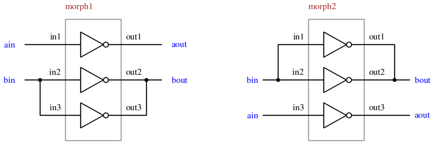
As you can see, the two circuits are equivalent, but the inputs
are connected to different inverters in the same cell. As far
as the netlist is concerned, the three inverters are identical,
and indistinguishable. This makes the netlist of the two
subcells "triinvert" have multiple symmetries. If you run LVS
on these two files, the terminal output will report:
Circuits match with 4 symmetries.
Netlists match uniquely.
Circuits match correctly.
However, when it comes time to compare the two top-level cells,
the symmetries are fixed; this happened at the time of the output
line "Netlists match uniquely". Symmetries imply non-uniqueness.
But the two subcircuits in the two netlists have pins, and those
pins have unique names that break the symmetry. Above the level
of that cell in the hierarchy, the pins "in1" and "out1" are
treated as specific pins of the subcircuit "triinvert", and cannot
be viewed as permutable with "in2" and "out2", or with "in3" and
"out3". (Side note: The "permute" command would not be useful
in this context, as it only works for individual pins, not groups
of pins. Making all the "in" pins permute and all the "out" pins
permute would be completely wrong, as netgen would no longer be
able to see the difference between a signal that entered on "in1"
and exited on "out1" in one netlist but entered on "in1" and
exited on "out2" in the other.)
So these two circuits use the three inverter resources in the
subcircuit "triinvert" differently, and so the netlist fails.
Once this has been determined as the failure mechanism, however,
it is relatively easy to fix, by flattening all instances of
"triinvert" so that the pins which break the symmetries are
removed. The setup file "setup_tut8b.tcl" does this
flattening, so that if you run the script "runtut8b.sh",
the symmetry is kept up to the top level and the two circuits
are declared matching.
It would be preferable if netgen could detect such group
symmetries and selectively flatten accordingly. Unfortunately
it does not do so at this time, but it is a topic for future
development.
Download the set of files in tut9. If you look at the two
files to compare, x.spice and y.spice, you will see
that x.spice has two device lines, one of which uses the
SPICE parameter "M = 2"
to declare two parallel copies of the device, while the file
y.spice has two parallel devices explicitly declared.
Run the script runtut9.sh and look at the output file,
comp_tut9.out. Note that in the subcircuit summary, both
sides claim to have two PMOS devices. What netgen does is to
expand out any use of "M =" in a
netlist into individual devices.
At this time, netgen is unable to sort out differences in number
of devices that may be a tradeoff with a property such as width
and/or length. That is a topic for future development.
There are occasions when a correct netlist will not be able to pass
LVS due to unexpected mismatches in the hierarchy. For example, a
resistor network in two cells may contain a subcircuit with four
resistors (let's call it "res_array") and an additional lone
resistor not in a subcircuit. Both circuits have the same name
("res_array") for the subcircuit containing the four resistors,
so those two subcircuits are matched and pass LVS. However, each
netlist makes different connections to those resistors. To the
LVS tool, each circuit has one instance of "res_array" and one
resistor device, so they appear to be matched; but these have
different network connectivity in each cell, so the LVS fails.
Depending on the circumstance, the end-user may want this
situation to fail LVS, such as if the resistors in "res_array" are
in a special layout with best-matching practices, and using the
lone resistor instead of one in the array would be considered an
error.
In the case that it is known not to be an error, the LVS can be
made to pass by specifically forcing netgen to flatten the resistor
array in both circuits, in setup.tcl:
flatten parent_cell {res_array file1}
flatten parent_cell {res_array file2}
Note that this use requires netgen version 1.5.53 or newer.
Previous versions would only allow "flatten
{res_array file1}", which would flatten all
instances of res_array in the
whole file, not just within the cell parent_cell
. That works, but at the expense of losing a level
of hierarchy in cells where it was not necessary to do so.
In general, properties are compared where both netlists define them
for a cell, instance, or (low-level) device. If only one of the
netlists defines a property, it is assumed to be meaningful only to
that netlist (e.g., relevant to layout or schematic, but not both),
and no warning is issued about missing properties in the other
netlist. Sometimes, however, properties exist in both netlists
but are often in disagreement not due to an error in the netlists,
but due to the way different tools generate or use those values.
A typical example is the source and drain area and perimeter values
for MOSFET devices. In SPICE files, these are given the (fixed)
names "AD", "PD", "AS", and "PS". In cases where these are present
in both netlists, are often conflicting, and are generating large
amounts of unnecessary output, they can be supressed by deleting
them from one of the nelists:
property {file1 nmos} remove ad as pd ps
property {file1 pmos} remove ad as pd ps
where "file1" is the name of one of the netlist files. It is not
necessary to remove the parameters in both netlists, although it
is necessary to have one statement per device that defines those
properties.
It is generally best to avoid flattening netlists unless absolutely
necessary. Use hierarchical netlists whenever possible, and keep
the hierarchies the same between the two netlists. It will be much
easier to track errors when each cell has a handful of subcircuits
with pins instead of possibly thousands of devices. If a circuit
has to be flattened, use commands in the setup file to flatten only
those circuits for which it is needed (see above). Don't flatten
any cells until it becomes apparent that LVS will fail without it.
- November 24, 2007
- Placeholder created for netgen tutorial
- October 8, 2012
- Finally getting around to writing the tutorial. . .
- November 1, 2012
- Moving on to describing the examples.
- May 19, 2016
- Tutorials revised, improved, and expanded.

| email:
| 
|
Last updated: October 28, 2025 at 9:54am