Qflow Tutorial
Digital Flow Example
Verifying the Layout with Netgen
Simulating the Layout with iverilog
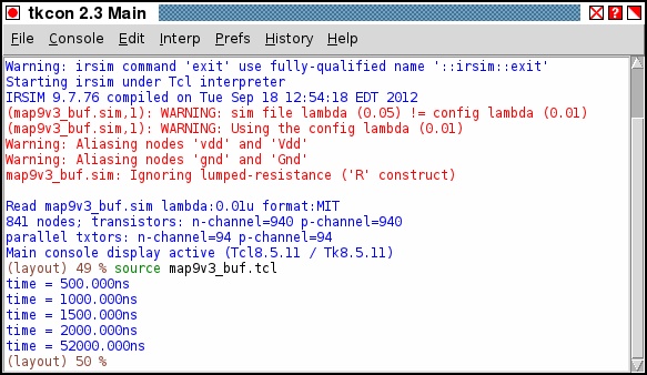
Simulating the Layout with IRSIM
Simulating the Layout with XSPICE
This tutorial runs through a complete synthesis example using the "standard" flow, which is command-line based. As of qflow version 1.1.104 (April 2018), most people will find the GUI-based flow, described in this tutorial more intuitive and easier to understand and to run. The GUI flow is based entirely on the command-line flow. In fact the GUI and command-line flows are essentially interchangeable. Not every option available to qflow has been put into the GUI, so for advanced use, it is likely that one or more steps may require the command-line use, for which the user will need to understand how to manipulate the setup files for each step. Also, the command-line version can be driven from a script or from a Makefile, for complete automation which the GUI version does not offer.
Download files for the example in the next section
map9v3.v is an example of a simple Verilog source file. It is a configuration logic block for a chip built by MultiGiG, and by itself it is absolutely useless, not to mention inscrutable, which is why it makes a good choice for an example. Note that I was going to use one of the verilog sources from the OSU standard cell library download, but it has multiple modules per file, and uses specific cell instances in the verilog. Such complications will be covered (eventually) in a separate tutorial.The Verilog subset understood by synthesis frontends such as yosys and Odin-II requires code that does not contain specific timing information (e.g., the "#" construct, although some limited forms of this are parsed and ignored). This reflects the difference between verilog used for simulation (testbench verilog) and verilog used for synthesis (synthesizable verilog). The verilog definition incorporates both styles, so one must be careful not to pass testbench-style verilog to a synthesis tool.
File Revision Size Date map9v3.v 1 2.0KB May 11, 2013 load.tcl 0 215B May 11, 2013 map9v3.tcl 0 306B May 11, 2013 map9v3.cel2 0 866B August 24, 2016 osu035_stdcells.gds2 0 339kB June 6, 2013 map9v3_gates_tb.v 0 717B April 28, 2015 osu035_stdcells.v 0 24kB April 28, 2015 setup.tcl 0 162B March 14, 2017 map9v3_cosim_tb.spi 0 953B June 6, 2017 NOTE: If you use qflow-1.4, some naming conventions for nets and pins were changed, so the following two files need to be used in place of the ones shown above:
The following is an example of a digital flow from Verilog source to layout.
File Revision Size Date map9v3.tcl 1 314B May 5, 2019 map9v3.cel2 1 954B May 5, 2019 Setup
Note that if you don't have these directories defined, qflow will still work, but it will inconveniently dump everything into the current working directory. Still, flat workspaces appeal to some. . .
- Install qflow-1.3 and all prerequisites mentioned on the qflow reference page. For the example, the default OSU035 technology can be used, so you don't need to download any additional tech libraries.
- Create a working directory somewhere in your workspace; for the purposes of the example, assume that the directory path to the example is held as a variable name called ${project_dir}, which will be used throughout the example to refer to the project top-level directory.
- Create three subdirectories of ${project_dir} called source, synthesis, and layout.
- Copy the example file map9v3.v to directory ${project_dir}/source.
All instructions in this tutorial will assume a directory structure like that indicated above.
Execution
From the project directory, run:qflow synthesize place route map9v3(Note: the above command is for qflow version 1.1 and newer; for qflow version 1.0, use "qflow synthesize place buffer route map9v3".)
This command creates three files in the working directory:qflow_vars.sh is a file containing information about the technology that is collected in one place and passed to each tool in the digital synthesis flow.Typically, one would run "qflow map9v3" without options, and then work through the steps of the flow by uncommenting each section, one at a time, and running the flow through that section, checking results, then moving on to the next section. Files needed for each section are saved in the working directories, so qflow can pick up where it left off in the previous step.
qflow_exec.sh is a file containing a sequence of commands to issue for the synthesis, placement, and routing. The simple qflow command without options other than the project name will cause all of the commands to be commented out.
project_vars.sh is a file that will be created once and never overwritten. It is where you would set specific options to fine-tune the synthesis flow to your needs. This tutorial will not cover much beyond the defaults, and you can ignore this file for now.
Results
This example has been vetted so that it should run to completion and give a routed result, assuming that all the tools have been installed properly.Power Bus Striping
Beginning with qflow version 1.1.54, qflow implements power bus striping. Because the power bus striping often requires selecting the right metal backend stack for the process, it is left undefined by default. This results in layouts that have isolated power and ground lines for each row. But because the OSU standard cell sets have a fixed metal backend stack and define all the routing layers inside the same file as the standard cell macros, automatic power bus striping is easy to set up. With any text editor, edit the file "project_vars.sh" in the project's top level directory. If you have an older version of qflow, there will not be any commented-out suggestions for options to pass to the tool "addspacers". But if you have qflow version 1.1.54 or newer, you will see the line:# set addspacers_options = "-stripe 5 200 PG -nostretch"Uncomment this line and change "200" to "100", because the cell is small and the power rails need to be closely spaced or they don't fit in the cell at all. The values passed after "-stripe" are stripe width, pitch, and pattern, respectively. The width and pitch are in microns (so, 5 micron wide power buses spaced 200 microns apart). The pattern represents how each row is connected, either "P" for "power" or "G" for "ground". Normally this is just "PG", which will alternate stripes between power and ground. The "-nostretch" option means that the power bus stripe will be run over the existing layout. Without this option, the cell will be stretched so that fill cells are under the power buses, making them (somewhat) less likely to get in the way of signal routes.Your entry in
project_vars.sh should look like:set addspacers_options = "-stripe 5 50 PG -nostretch"Once you have made this change, run qflow again, and the power buses should be automatically inserted and connected into the standard cells.
A synthesized circuit is supposed to be correct by design, but it is always a good idea to check the circuit both by LVS and by simulation.To run this tutorial, you will need to have the tool netgen 1.5 installed on your system. Make sure that it is compiled with Tcl/Tk support, or else you will have to refer to the netgen documentation for doing a comparison without using the "lvs" command.
After running qflow through the detailed routing, use Magic to read in the circuit. There is a limitation of the layout tool in which it understands of the cell bounding boxes defined in the LEF file for standard cell placement, but this understanding does not transfer to layout files in the standard database format. The best way to ensure that the physical layout view matches the abstract LEF view is to do the following:
- Magic will need access to the technology file for the process used by the OSU035 standard cells, which is the scalable-CMOS rules from MOSIS with a few modifications. The modified technology file is included with the qflow distribution. More recent revisions of qflow (from 1.0.13) will install a startup script ".magicrc" in the layout directory. This startup script is responsible for loading the correct technology file from the qflow install directory. For versions of qflow prior to 1.0.13, you will need to copy the techfile SCN4M_SUBM.20.tech from the qflow install directory (/usr/local/share/qflow/tech/osu035/) to the local layout directory.
- Start Magic, for example, "magic -d XR" in the layout directory (or just "magic" if you don't have libcairo support).
- Load the abstract LEF views, using:
lef read /usr/local/share/qflow/tech/osu035/osu035_stdcells.lefThere will be a number of warnings related to statements that the LEF reader in magic doesn't handle; these can be ignored.- Load the routed DEF file, using:
def read map9v3.def- If you wish to see the routing grid, use
grid 1.6um 2.0umAll of the steps from the "lef read" command up to and including the "grid" command are included in the script file "load.tcl" in the download sections at the top of the tutorial. If you downloaded this file, put it in the layout directory. Then, start Magic and type into the console:source load.tcland proceed from the next step.
- Save the top-level design. In this case, you do not want to save the abstract views, although it can be helpful to keep the database versions of the abstract files in a separate directory and use the "addpath" command (see below) to switch between the abstract and physical views. To write the database for just the top-level cell, do:
writeall force map9v3The circuit above was routed with qflow version 1.1.55 using power striping as described above, and routing on the first three layers only.
- Now quit Magic to lose the abstract cell views (say "Yes" to the prompt, you really do want to exit!)
- If you have downloaded the OSU standard cell set, skip this step and go to the next one. Otherwise, download the file osu035_stdcells.gds2 from the download list at the top of the page (put it in the layout subdirectory). I recommend downloading the OSU standard cell set from the OSU website to get the most up-to-date version. However, the version posted here will suffice for the tutorial.
Because there are a lot of standard cells, you may want to keep these layout views in a subdirectory of the layout directory, so from the layout directory, do:
mkdir digitalStart magic without specifying a file to load:
cp .magicrc digital
cd digital
magic -d XRThen load the GDS file, and save all of the standard cells:gds read osu035_stdcells.gds2Note that you may need to specify a complete path to osu035_stdcells.gds2 in the statement above for magic to be able to find the file. The set of commands above assumes that the GDS file has been placed in the digital subdirectory.
writeall force
quit
Now return to the layout directory. The .magicrc script already has an "addpath digital" command in it, so it will be able to find all the standard cell layout views. Skip the next step.
- If you have downloaded the OSU standard cell set, you will want to execute the "addpath" command to access the Magic database views of the standard cells. For example, if the OSU distribution was put under ~/osu, then the command would be:
addpath ~/osu/cadence/lib/source/magicThis statement can be added to the ".magicrc" script file so that it will be applied every time magic is run from the layout directory.
- Load the layout view of the project top-level, which will now reference the physical layout views, not the abstract LEF views:
magic -d XR map9v3- As mentioned at the top of the tutorial, qflow version 1.1.54 has an extended tool "addspacers" that automatically inserts and connects power and ground across all rows of the layout. If you have this version of qflow and have added the proper options to the project_vars.sh file, then the layout will have two wide stripes down the middle in metal4 that fully connect power and ground, as shown in the screenshot below. This makes life a lot easier, and you can skip the rest of this step and proceed to the next. Otherwise, continue reading below.
Once again, please note that the instructions from here to the end of this entry are for earlier versions of qflow that do not have automatic generation of power bus striping. If you are missing two wide vertical metal lines down the middle of the layout, then the power buses are not connected together, and you will need to follow the instructions below.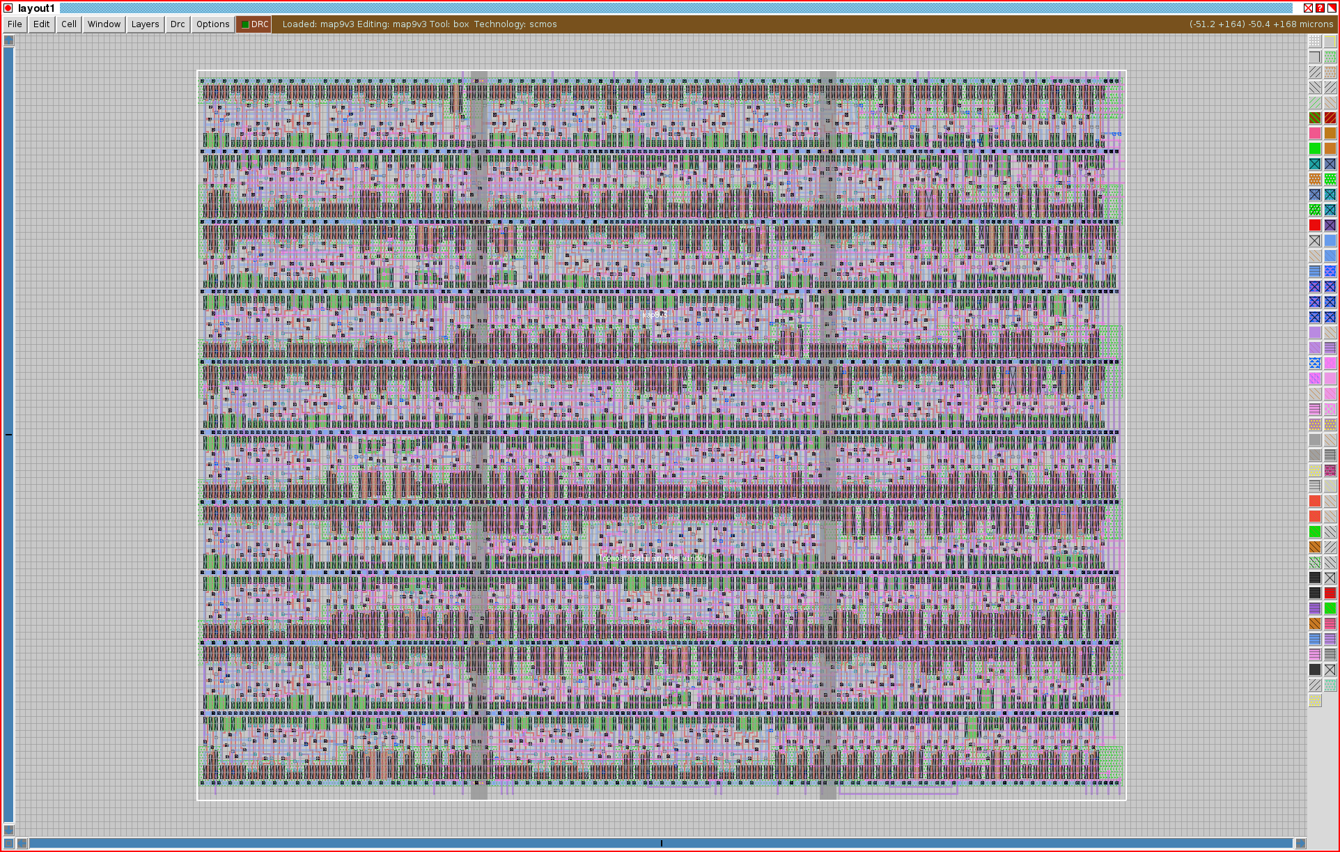
Earlier versions of qflow do not place power buses. To make sure that all the vdd and gnd rows on the standard cells are connected, use the magic layout editor to extend the vdd metal1 lines out to the right and connect them vertically with metal1 (easiest) or metal2; do the same on the left with the gnd metal1 lines. Then, put the cursor box on the vdd metal1 bus and type
label vdd n m1And similarly, putting the cursor box on the gnd metal1 bus, typelabel gnd n m1and then save again usingwriteall force map9v3The layout should now be a valid, operable digital circuit. It may not look exactly like the picture above, depending on the option choices (this picture is updated occasionally to keep up with recent versions of qflow, but sometimes the behavior differs. The picture above is from a run with a fixed height of six rows, so the aspect ratio is different from what you would get using default settings).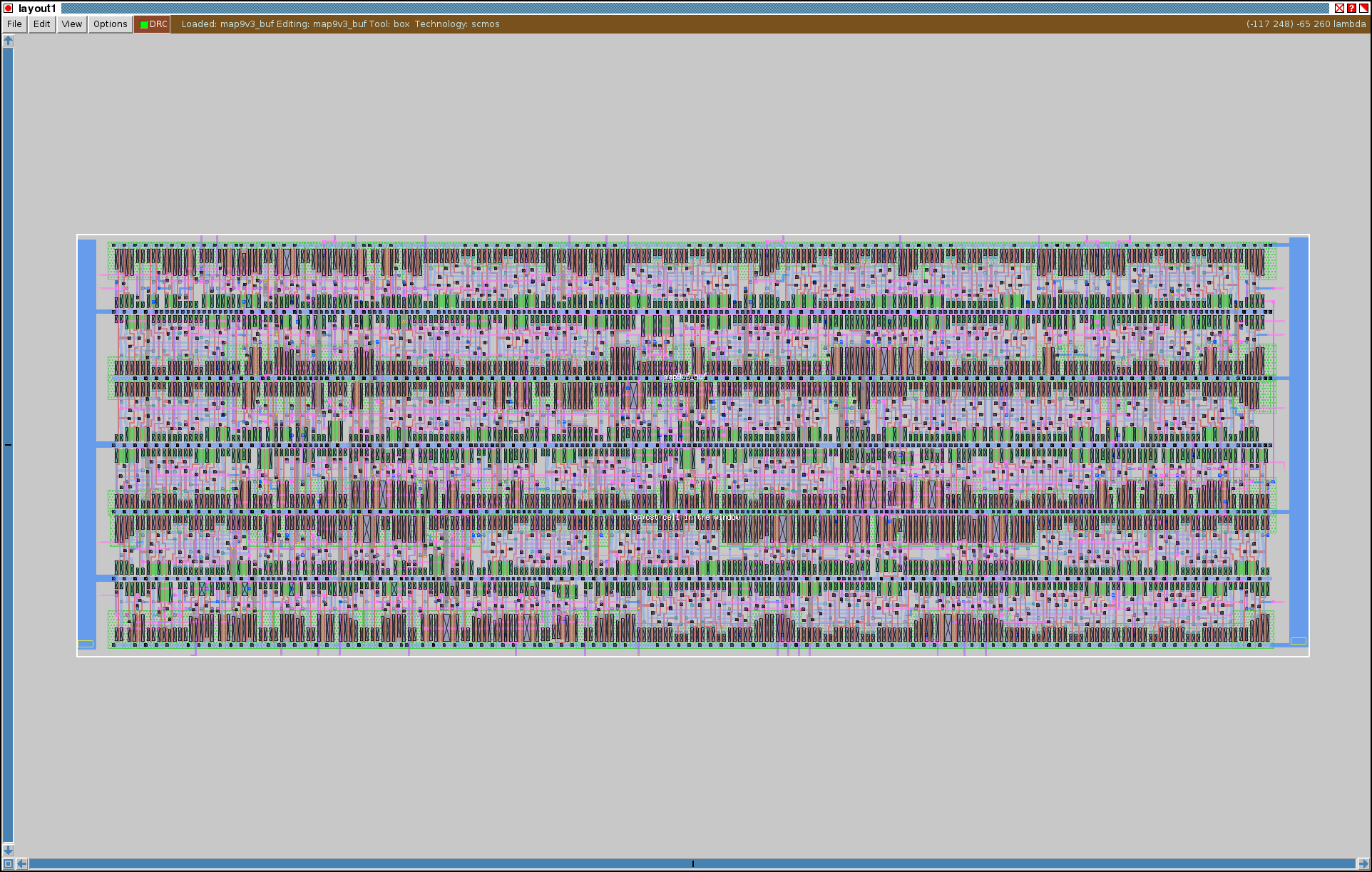
- Generate a SPICE netlist from the design using the following sequence of commands:
extract allThis step will produce a file "map9v3.spice", a hierarchical description of the circuit down to the transistor level. It is the physical view, extracted from the connectivity of the wires. We want to compare it with the original netlist produced by the synthesis.
ext2spice hierarchy on
ext2spice scale off
ext2spice renumber off
ext2spice cthresh infinite
ext2spice rthresh infinite
ext2spiceNote that the use of "cthresh infinte" and "rthresh infinite" disables the generation of parasitic devices, which are not wanted for LVS comparison; otherwise you get capacitor ("c") devices in the layout netlist that are not matched in the schematic netlist.
- While you're at it, also create the .sim format file for the IRSIM simulation described below. Use the command
ext2sim- Quit Magic---its job is done.
- The Qflow synthesis and resynthesis scripts generate a SPICE netlist directly from the BLIF format netlist, so this is what we want to compare against. It is found in the synthesis subdirectory, and has the name "map9v3.spc".
- Download the file "setup.tcl" from the downloads list above, and put it in the project top-level directory. This is the file that tells netgen important information about the technology and the standard cell set. In particular, it is needed to avoid counting the filler cells in the layout as something needing to match the schematic.
- From the project top-level directory, run netgen version 1.5:
netgen- The SPICE netlist generated from the BLIF netlist uses the SPICE netlists for the standard cell subcircuits directly from the standard cell distribution. These will be compared against the extracted standard cell circuits from the layout. While the layout views that were read from the standard cell distribution are expected to match the netlists from the same distribution, this is a good check against errors in scaling, failure to tap wells and substrate, or formatting errors in general.
Even if the standard cells match, we have to deal with the discrepancy between the way the SPICE netlists are formatted. The extracted view has no information about ports, as the circuit would need to connect to something at a higher level (such as a chip top level). The SPICE netlist generated from the BLIF netlist and standard cell netlist library, on the other hand, has all the port information for the top-level cell and generates a ".subckt" record for it. The way to handle this in netgen is to call the "lvs" command with a list for the second circuit containing the filename of the SPICE netlist, and the name of the subcircuit (see below).
Since both the extracted circuit and standard cell netlist library are expected to refer to the same set of device models, both SPICE netlists should use the same names for low-level components (e.g., "nfet" and "pfet").
The command to run in netgen is:
lvs {layout/map9v3.spice map9v3} {synthesis/map9v3.spc map9v3}Note that magic's behavior with respect to ext2spice changed in version 8.1.166. Prior to that, the default behavior was to dump the contents of the layout into a top-level netlist. With no .subckt line, there was no way to specify which nets were pins, so pins could not be compared between the subcircuits. In that case, there is no subcircuit name to specify for the layout netlist, and the call to run LVS is:lvs layout/map9v3.spice {synthesis/map9v3.spc map9v3}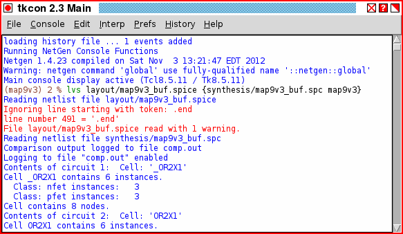
- Again, if everything has gone according to plan, then the last two lines of output from netgen should be:
Result: Circuits match uniquely.If this does not happen then a detailed report of the LVS errors will be dumped into a file called comp.out. It is worth taking a look at the comp.out file anyway, to see a summary of the comparison.
LVS Done.For example, a failure to extract without parasitics will result in a netlist mismatch with the layout device showing many capacitor devices that are not present in the schematic view.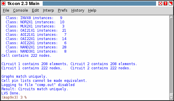
Note that netgen can be called entirely from the command line, without the console, using the form:
netgen -batch lvs "layout/map9v3.spice map9v3" "synthesis/map9v3.spc map9v3"(And likewise, if the version of magic is prior to 8.1.166, then there is no subcircuit definition in the layout netlist, and the correct syntax is 'netgen -batch lvs layout/map9v3.spice "synthesis/map9v3.spc map9v3"'.)
LVS netlist comparison is only a check for the internal consistency of the placement, and routing of a design (which is itself complicated and therefore prone to error, even in expensive commercial tools). But the LVS compares the layout against the schematic generated by the synthesis stage, and so it says nothing about the functional validity of the gate-level netlist. It is wise to do functional verification of the gate-level netlist with a verilog simulator. Because qflow generates a gate-level verilog netlist as a synthesis output, it is easy to run a verilog simulator on both the original verilog source code and the structural (gate-level) verilog netlist.Note that prior to version 1.0.94 (April, 2015), the structural verilog netlist "project_name.rtlnopwr.v" could contain undefined references to "vdd" and "gnd", and to simulate correctly would need the additional verilog statements "wire gnd = 1'b0;" and "wire vdd = 1'b1;" added to the netlist by hand. From qflow version 1.0.94, these two statements are automatically written to the output file.
Download the verilog testbench "map9v3_gates_tb.v" from the download section above. Also, you will want the verilog of the standard cells ("osu035_stdcells.v"), which you can download from the section above, get from the OSU standard cell download, or from the installed techfile directory in qflow (by default, /usr/local/share/qflow/tech/osu035/osu035_stdcells.v) (and thanks to Leandro Marsó for converting the original IRSIM testbench into verilog!).
The structural verilog can be simulated in any verilog simulator; Icarus verilog ("iverilog") is a good choice, and the one I recommend. To run the testbench, you will just need to pass to iverilog the three verilog files needed: The standard cell definitions, the gate netlist, and the testbench:
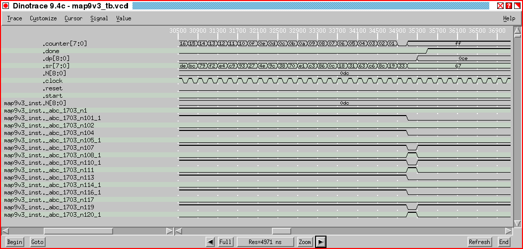
iverilog osu035_stdcells.v map9v3.rtlnopwr.v map9v3_gates_tb.vIcarus verilog is a compiler, so by default it generates an executable called "a.out", which must be run to obtain the testbench output:./a.outThis testbench generates an output file "map9v3_tb.vcd", if you want to look at waveforms using a waveform viewer (such as gtkwave or the older dinotrace, shown below). However, it also generates diagnostic output that is enough to show that the circuit is working as expected:VCD info: dumpfile map9v3_tb.vcd opened for output.The last line in the output above shows the first latched value in dp, which is (decimal) 206, and is the expected output. The waveform view of map9v3_tb.vcd using dinotrace is shown below.
At time 0, counter = 00 (0), sr = 00 (0), dp = 000 (0)
At time 530000, counter = 94 (148), sr = 00 (0), dp = 000 (0)
At time 550000, counter = 93 (147), sr = 01 (1), dp = 000 (0)
... At time 3490000, counter = 00 (0), sr = 33 (51), dp = 000 (0)
At time 3510000, counter = ff (255), sr = 67 (103), dp = 000 (0)
At time 3530000, counter = ff (255), sr = 67 (103), dp = 0ce (206)
...
I mentioned above that running a verilog compiler/simulator like icarus will verify the function of the original source code and/or the gate-level netlist produced by the synthesis tool. A layout-vs.-schematic (LVS) tool will show a topological equivalence between the gate-level netlist and the layout. Generally speaking, the two of those together are sufficient to prove the validity of the layout.In the end, however, you may want to ensure the correctness of the physical layout directly, by a simulation at the lowest (i.e., transistor) level, in particular to be done with an extracted netlist containing a (reasonably accurate) estimation of parasitic capacitances and resistances in the physical layout.
The best way is to extract a ".sim" netlist from Magic (see above), and simulate using IRSIM. IRSIM (see the IRSIM website on opencircuitdesign.com) has commands that make it very easy to construct a simulation that exactly matches a Verilog testbench. So you can simulate through IRSIM and check the results in the analyzer against the output of, say, iverilog and dinotrace. Another way is to extract the SPICE netlist from Magic and simulate using a SPICE simulator such as ng-spice (note that such a SPICE netlist will differ from the one generated above for the netgen LVS, because the netlist for LVS does not contain parasitic devices). However, SPICE simulation, while very accurate, does not scale very well with size; a moderately complicated verilog module can end up taking hours, days, or even weeks to simulate in SPICE. IRSIM, by contrast, works at the same base level of components like transistors, resistors, and capacitors, but with simplified models that strike a good balance between accuracy and simulation performance.
- For convenience, copy the IRSIM parameter file from the qflow technology directory to your layout directory:
cd layout
cp /usr/local/share/qflow/tech/osu035/osu035.prm .
- Download the IRSIM command file "map9v3.tcl" from the download list above, and also place that in the layout directory.
- Run IRSIM using:
irsim osu035.prm map9v3.sim- Once the IRSIM command window is up and the netlist has been loaded in, run the testbench simulation by typing into the console:
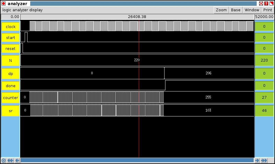
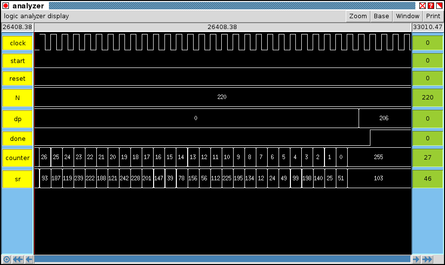
source map9v3.tcl- The script should automatically generate the logic analyzer window. Expand to the full view of the simulation by clicking on the target icon in the lower left-hand corner of the analyzer window. What you should is is that in the simulation, the circuit is given a start pulse, the counter and shift register start changing every clock cycle, and after about 100 clock cycles, the "done" signal goes high and the output "dp" is latched. The simulation uses an input value N of (decimal) 220 and should get as output a value for dp of (decimal) 410. If you see these values, then the circuit has been (minimally) functionally verified!
Ultimately, a circuit like this example which is meant to be used in a mixed-mode (analog and digital) system needs to be simulated in a full analog simulation, that is, SPICE. It is an inherent limitation of SPICE that fast signal edges will slow it down, and digital systems being basically large collections of fast switching signals will slow SPICE down to a crawl.A event-based co-simulation environment called XSPICE was developed for SPICE to overcome this problem by providing a way of simulating digital circuits at the level of logic gates, without incurring the high overhead of transistor-level simulation of digital logic functions. XSPICE was developed in Berkeley SPICE3, and is part of ngspice if it happens to be compiled in. Oddly, XSPICE has not received the attention it deserves. Part of the reason is the implication that XSPICE models must always be written in C and compiled into SPICE. The set of digital models bundled with the XSPICE source was not complete enough to represent a usual digital standard cell set. However, it had flip-flops, latches, and an assortment of gates. All it needed was a way to represent arbitrary combinational logic functions, without requiring a new device model to be written in C every time a new function was implemented in the standard cell set. So I wrote an extension to the XSPICE set of models called "d_lut" and "d_genlut" which do just that: They can encode any arbitrary combinational logic expression as the output of a lookup table (LUT). To make use of this, only the "d_lut" and "d_genlut" models need to be compiled in C, and for that, you will need a version of ngspice supporting it. The current version of ngspice on sourceforge, as of this writing (2018), which is ngspice-27, has this extension.
I wrote a script called "spi2xspice.py" in the qflow source that reads a Liberty-format file describing a standard cell set and a SPICE netlist of a circuit made of standard cell logic, and produces a netlist with all digital gates represented by XSPICE primitives, using the original primitives for flip-flops and latches, and the new LUT models for all combinational gates. Versions of qflow from 1.1.51 will automatically generate an XSPICE netlist (requiring python3 to run the script). Qflow does not check the version of ngspice, but of course ngspice with the LUT models in XSPICE is needed to correctly simulate using the XSPICE netlist.
Warning: Most distributed versions of ngspice still don't have my xspice extensions. Make sure when you run ngspice it says it's ngspice-27 (or higher). If compiling from source, be sure to enable xspice when running "configure". If you don't have version 27, you will get a flatlined output from the circuit, and error messages at the top of the run that look something like this:
Model issue on line 255 : .model d_lut_clkbuf1 d_lut (rise_delay=1n fall_delay=1n ...The XSPICE netlist (which has an extension ".xspice", and is placed in the "synthesis" directory) is a direct drop-in replacement for the subcircuit in any compatible SPICE simulation. The circuit will simulate in what is, of course, a simplified manner, not proper for validating digital timing, but very fast and quite appropriate for functional simulation of a mixed-signal system.
Unknown model type d_lut - ignored
Download the SPICE testbench "map9v3_cosim_tb.spi" from the download section above. This testbench uses SPICE primitives (namely independent voltage sources) to power the device under test and apply clock, reset, and start signals, and to apply the input value. It uses the ngspice control block to run a transient simulation and plot the main control signals. The control signal plot from the XSPICE simulation is shown below.
For comparison, replace the "include" statement at the top of the SPICE testbench file with the transistor-level SPICE netlist "map9v3.spc" and re-run the simulation. This will show that the XSPICE netlist is indeed a drop-in replacement for the transistor-level netlist, and also will show just how much performance improvement is gained by using the XSPICE models (you may not want to wait around for the transistor-level simulation to finish!).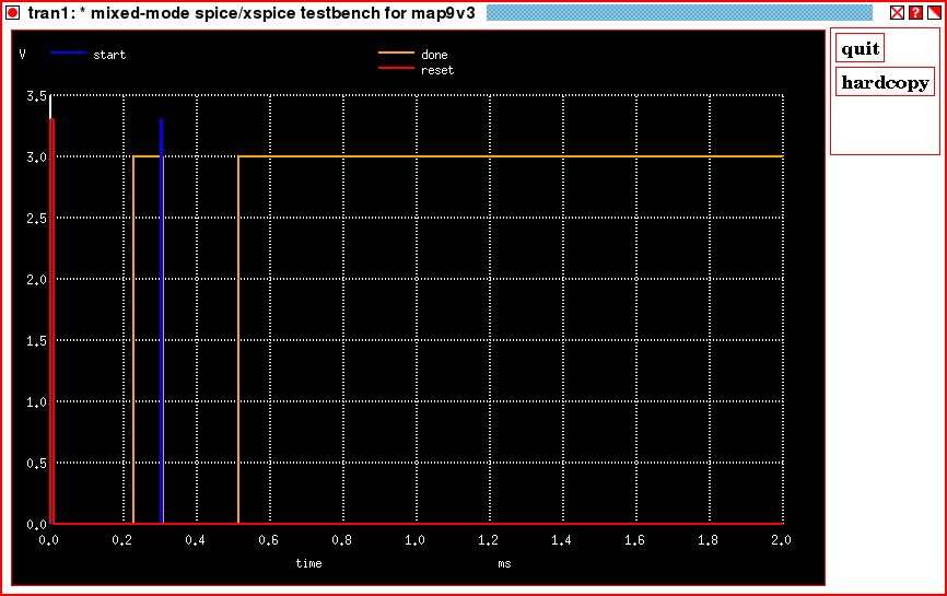
![]()
| email: | 
|
Last updated: October 28, 2025 at 9:47am