 Qflow 1.3 Digital Synthesis Flow Tutorial Page
 Qflow 1.3 Digital Synthesis Flow Tutorial Page
Qflow (GUI) Tutorial
Digital Flow Example
Simulating the Design
Pin Placement Hints
This tutorial runs through a complete synthesis example using the GUI-based flow. Introduced in qflow version 1.1.104 (April 2018), most people will find the GUI-based flow intuitive and easier to understand and to run than the standard command-line flow. There are several reasons to use the standard flow instead of the GUI: Not every option available to qflow has been put into the GUI, and the command-line version can be driven from a script or from a Makefile for complete automation which the GUI version does not offer. The standard command-line flow is described in this tutorial. For the user just wanting to get circuits synthesized, placed, and routed; or just wanting to understand how digital synthesis works, the GUI is a much easier platform to start from.
Download files for the example in the next section
map9v3.v is an example of a simple Verilog source file. It is a configuration logic block for a chip built by MultiGiG, Inc., many years ago, and by itself it is absolutely useless, not to mention inscrutable, which is why it makes a good choice for an example.The Verilog subset understood by synthesis frontends requires code that does not contain specific timing information (e.g., the "#" construct, although some limited forms of this are parsed and ignored). This reflects the difference between verilog used for simulation (testbench verilog) and verilog used for synthesis (synthesizable verilog). The verilog definition incorporates both styles, so one must be careful not to pass testbench-style verilog to a synthesis tool.
File Revision Size Date map9v3.v 1 2.0KB May 11, 2013 The following is an example of a digital flow from Verilog source to GDS mask output.
Setup
- Install qflow-1.1.104 or newer and all prerequisites mentioned on the qflow reference page. For the example, the default OSU035 technology can be used, so you don't need to download any additional tech libraries.
- Create a working directory somewhere in your workspace; for the purposes of the example, I will assume that this is your current working directory, and is initially empty.
- You may copy the example file map9v3.v to the current working directory if you do not have it elsewhere, but this step is optional. You will need to know the location of your verilog source file.
Execution
From the project directory (that is, "cd" to the project directory), run:qflow gui(Note: the above command only works for qflow version 1.1.104 and newer!)
There are several ways to invoke the qflow GUI, none particularly preferred over any other. The path to the verilog file can be specified on the command line, as can the technology to use (the invocation would be "qflow -T technology verilog_file"; for example, "qflow -T osu035 ~/Downloads/map9v3.v"). Both the source file and target technology can be controlled through the GUI, which is how this tutorial is presented.
The GUI Window
Here is what the qflow GUI window looks like on startup using the above command ("qflow gui", from the command line):To explain the GUI: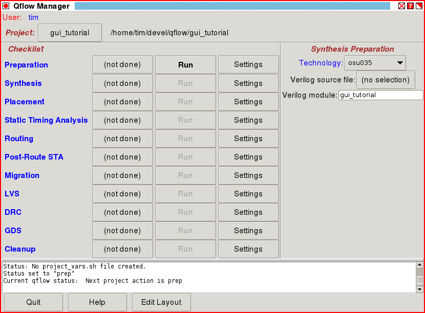
At the top is the "Project" name, which shows the working directory where the project files are kept. The working directory name is considered the name of the project (not to be confused with the name of the top-level verilog module). The full path to the directory is shown to the right of the button.Below the project name are two sections, the "Checklist" on the left side and the Settings window on the right. The Checklist is a list of steps proceeding through the synthesis flow, starting from preparing the workspace all the way to generating a GDS output file and cleaning up unneeded working files.
Beside each step in the Checklist are three buttons. The leftmost button shows the status of the step, from "(not done)" to "Okay" to "Fail", depending on whether or not the step has been completed, or showing the result of the step. Clicking on this button gives further details by displaying the log file for that step, which is mostly useful only if the step failed.
The middle button is the execution button and either says "Run" to run the synthesis flow step, or "Stop" if the step is running. The item that is next to run in the flow will have "Run" in boldface. Those steps ahead which cannot be run until other steps have run first will be disabled (grayed out). Steps which have already been run display "Run" in normal type. It is always possible to go back and re-run a step that has been run previously.
The button on the right is the "Settings" button. This controls what is displayed in the Settings window on the right, which is different for each step. Normally, the display in the Settings window corresponds to the next step in the flow to run. However, by clicking on the button, you can review the settings for any step of the process.
The Settings window is, as mentioned above, different for each step. Each window shows the settings that the user can control for that step. Settings can be changed at any time, although settings changed for a step after the step has been run will not apply until that step is run again.
Setting up for synthesis
Because qflow was started as "qflow gui" and with no other options, qflow starts in an unitialized state. The step is set to "Preparation", where the user can control what the input source to the synthesis is, and what technology to target. The default technology is "osu035", from the set of technologies bundled with and installed with qflow. There is no verilog source file, and the module name is just set to the name of the project, which is the name of the current working directory.So the first two steps (in any order) are to set the verilog source file and the technology. For technology, either keep the default or choose "osu018" ("osu050" does not have enough metal layers to automatically route power buses, and "gscl45nm" does not have all the files needed to run the full tutorial).
If you click on the "Verilog source file:" button, you will get a dialog window requesting you to select a file. Since this window starts in the current working directory, if you have put your verilog source file "map9v3.v" there, it should show up in the window, and all you need to do is click on it and click "Open". If you have the source file elsewhere, you will need to navigate through the file system and find it. Once you have selected the file and clicked "Open", the name of the file will appear in the button, and the module name will be set to "map9v3".
Note: If a verilog file has only one module defined in it, the module is set automatically. If the verilog file has more than one module but one of the modules matches the source file root name, then it will be set automatically. If in any case the module name is not the module intended to be the top-level module, enter the name of the top level module in the entry field next to "Verilog module:" before running the Preparation step.
Running synthesis flow steps
Now that the technology and source file have been specified (these are the settings for the "Preparation" step), click on the boldface "Run" button.This should end in the state shown below, with "Okay" showing in the status button for "Preparation", and the "Run" button for step "Synthesis" in boldface, indicating the next step to run.
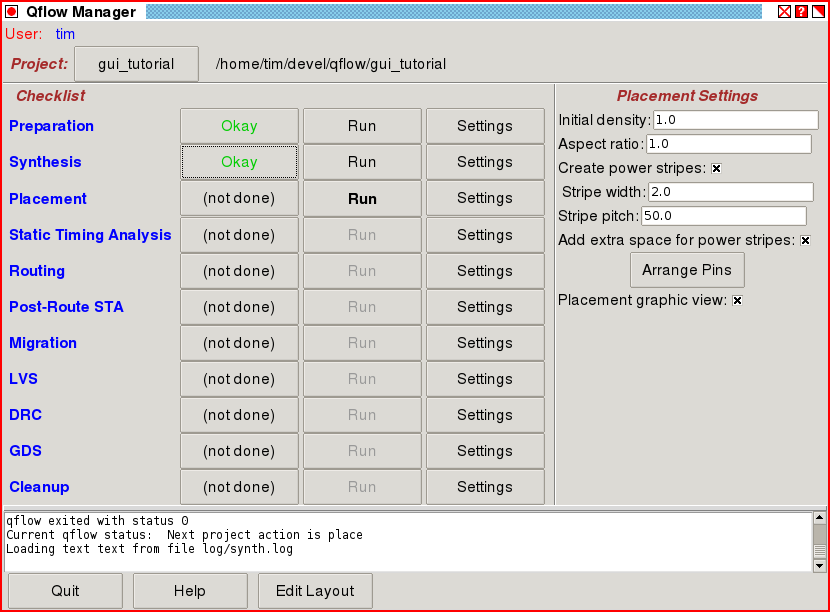
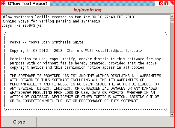
So far, there is very little user intervention in the process. Now click on the "Run" button for the Synthesis step. The GUI view should look like this: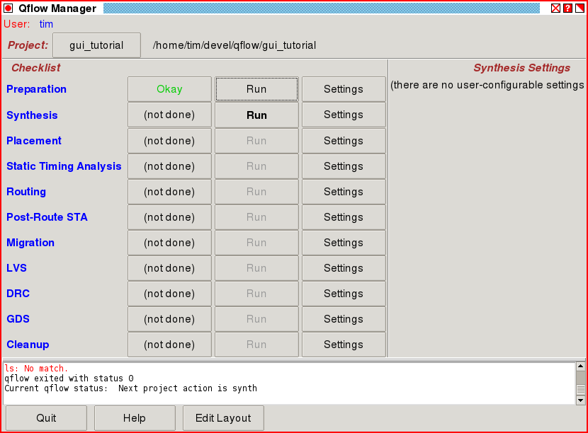 Before looking at the settings that can be modified for the placement process, click on the "Okay" button next to Synthesis. This brings up a window showing the contents of the synthesis step log file, as shown below:
 Click on "Close" to dismiss the window.
For "Placement Settings" in the window to the right, several controls over the synthesis process are available:
Click on the "Run" button to run the placement tool. If all goes well, then continue down the checklist, running each step at a time. Each step can only be run if the previous step has passed. The tutorial source verilog code has been chosen for its small size, so there should be no difficulty running any of the synthesis steps, and there should be no failures.
- Initial density:
- A value lower than one pads the layout with fill cells, lowering the density of the routed standard cells and making the layout easier to route, at the expense of overall layout area. Note that for small designs the size of the one in this tutorial, the design can be routed at full density (1.0).
- Aspect ratio:
- Change the aspect ratio of the design. Numbers greater than one result in a taller, narrower layout, while numbers less than one result in a shorter, wider layout.
- Create power stripes:
- This option is checked by default, meaning that power buses will be connected together with vertical metal wires. As mentioned earlier, this does not work for the OSU050 technology due to the limited number of metal layers available, but it works for all other technologies. (Generally, metal1 will be taken up by the standard cells, so metals 2 and 3 will be for vertical and horizontal routing. Since it is difficult to ensure that no pins are directly under the power bus, metal 2 cannot be used for that purpose, while metal 3 is horizontal. So four metal layers are the minimum needed for power striping. For three metal layers or less, the power buses will need to be connected up by hand, usually on the metal1 layer with a "comb"-like layout.)
- Stripe width:
- When making power stripes, each stripe will be this wide (value in microns). This value is generally set by the technology setup to be appropriate for the technology used.
- Stripe pitch:
- When making power stripes, the distance between stripe centerlines will be this amount (value in microns). Like stripe width, this value is generally set by the technology setup to be an appropriate number.
- Add extra space for power stripes:
- When checked, this option adds approximately as many fill cells as needed to cover the additional space used by the power buses. Note that given the different widths of standard cells, it may not be possible to put the fill cells directly under the power bus. However, the fill will be placed as close as possible to minimize the number of standard cell pins directly under a power bus, which can affect routability. This option is recommended for smaller cells because the power stripes take up proportionally more of the total layout area. For larger cells, the additional space is generally not needed.
- Arrange Pins:
- Pins can be arranged around the cell as required for floorplanning. This interface is its own topic; see below. For the purposes of the tutorial, it is not necessary to place restrictions on the pin placement.
- Placement graphic view:
- The placement will run somewhat faster if the graphic view is not displayed, although the overhead is low compared to the compute time for the placement algorithm itself, so generally this will be left checked.
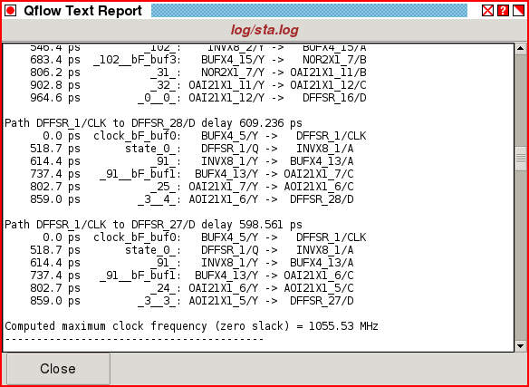
At any time after the "Placement" step has been run, the button "Edit Layout" at the bottom of the manager GUI window may be used to start the Magic layout editor to review the layout that has been made by the synthesis process. Up until the last step, the view will show the abstract (LEF) view of the standard cells. Prior to routing, of course, no routes will be in the layout. This is what the tutorial layout looks like after placement, when using technology OSU018 and using default settings for the Placement step:
After running the "Static Timing Analysis" step, click on the "Okay" button to review the static timing analysis results. For the OSU018 process, these results look like the picture below: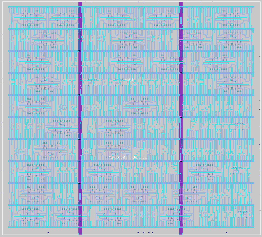 This shows the circuit operating at over 1GHz (this circuit was designed for high speed, having very short combinational chains between registers). Note that this is an artificially elevated number, as it does not consider delays caused by routing. That will be reported later, after the "Post-Route STA" step (which, by the way, is still over 1GHz, although a slightly lower number than before routing).
The "Migration" step is the first step since "Preparation" that is not a part of the core qflow command-line-driven scripts. The purpose of "Migration" is to convert the DEF file layout produced by Routing into a database for Magic, where the layout can be manipulated to avoid errors in LVS or DRC. Normally there will not be LVS errors, but one clear exception is the use of OSU050 mentioned above, in which the layout needs to be edited to connect the power and ground buses together on metal1.
An improperly defined setup is a good way to get LVS errors, although bad setups usually do not make it past the Routing step. Problems with offsets from the routing tracks or incorrect via definitions can often be determined by looking at the post-placement or post-routing layouts.
DRC errors will show up occasionally in spite of qrouter's best efforts to avoid them. Certain technologies have more difficulties with keeping the layout DRC clean than others. Magic runs its own interactive design rule checker, and any errors can be found using the "drc find" command, and eliminated by editing the layout by hand.
NOTE: The DRC is normally run using abstract views of the standard cells to keep the DRC runtime lower. However, the OSU050 standard cells have unusual abstract views that contain bits of metal that are intended to guide the routing, but are themselves in violation of DRC metal width rules. In this case, it is necessary to select the option "Use GDS view of standard cells:" to avoid the DRC issues caused by the abstract cell views.
The routed layout of the tutorial in OSU018 looks like the following:
Note that the LVS, DRC, and GDS steps are all not part of the core qflow command-line scripts, and require the installation of Magic and Netgen. In the final step, the GDS mask data file is generated. After the GDS file is available, the "Edit Layout" function will show the completed layout with full (not abstract) cell views, with the layout being read directly from the GDS output file. As a consequence, editing and saving the layout changes the Magic database, not the GDS file, so all edits should be completed before running the GDS step.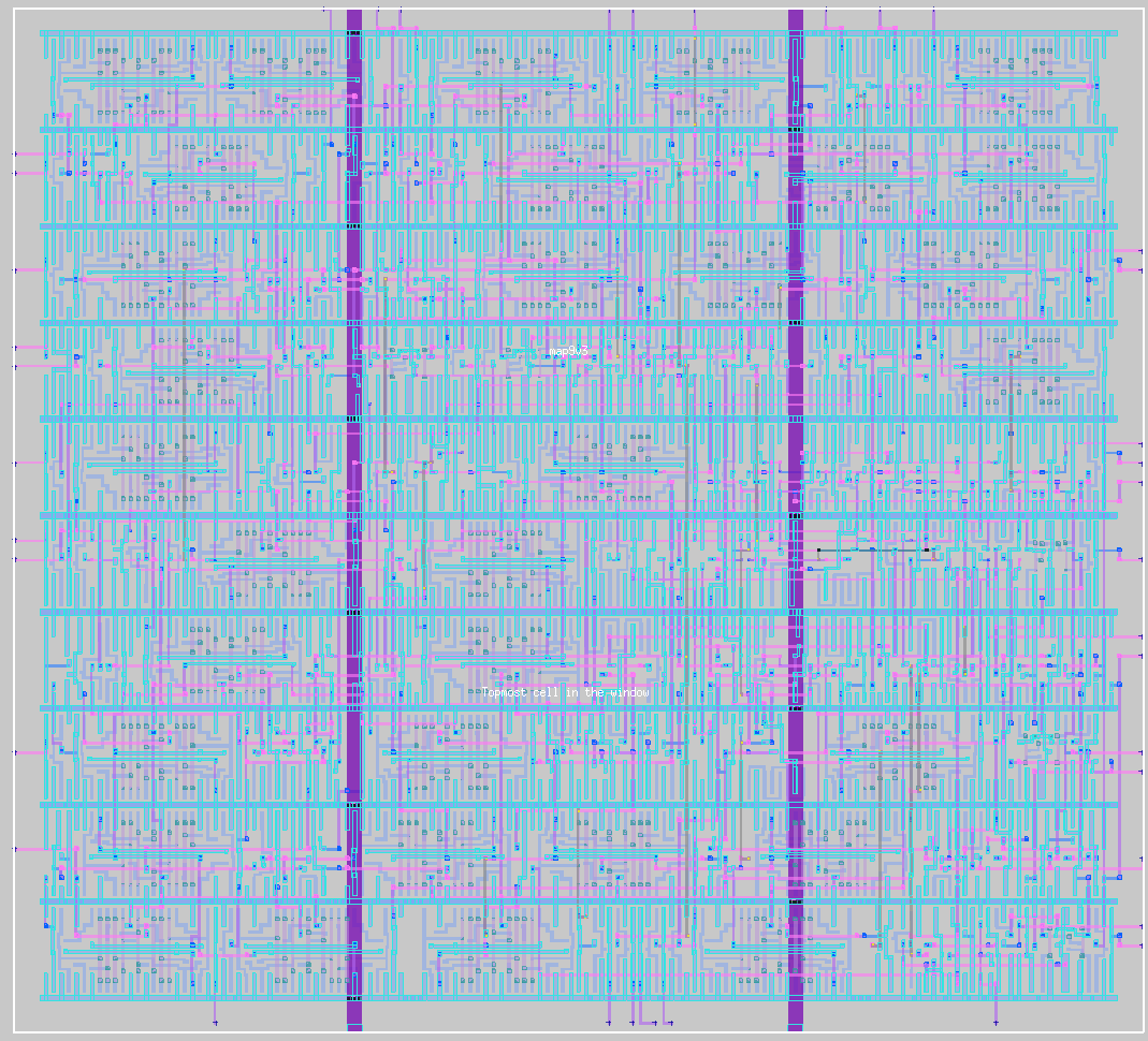
The completed layout looks like the following:
The final step is "Cleanup", which clears all unneeded files out of the workspace. All critical files are retained, so that the synthesis flow can still be re-run from any point in the flow.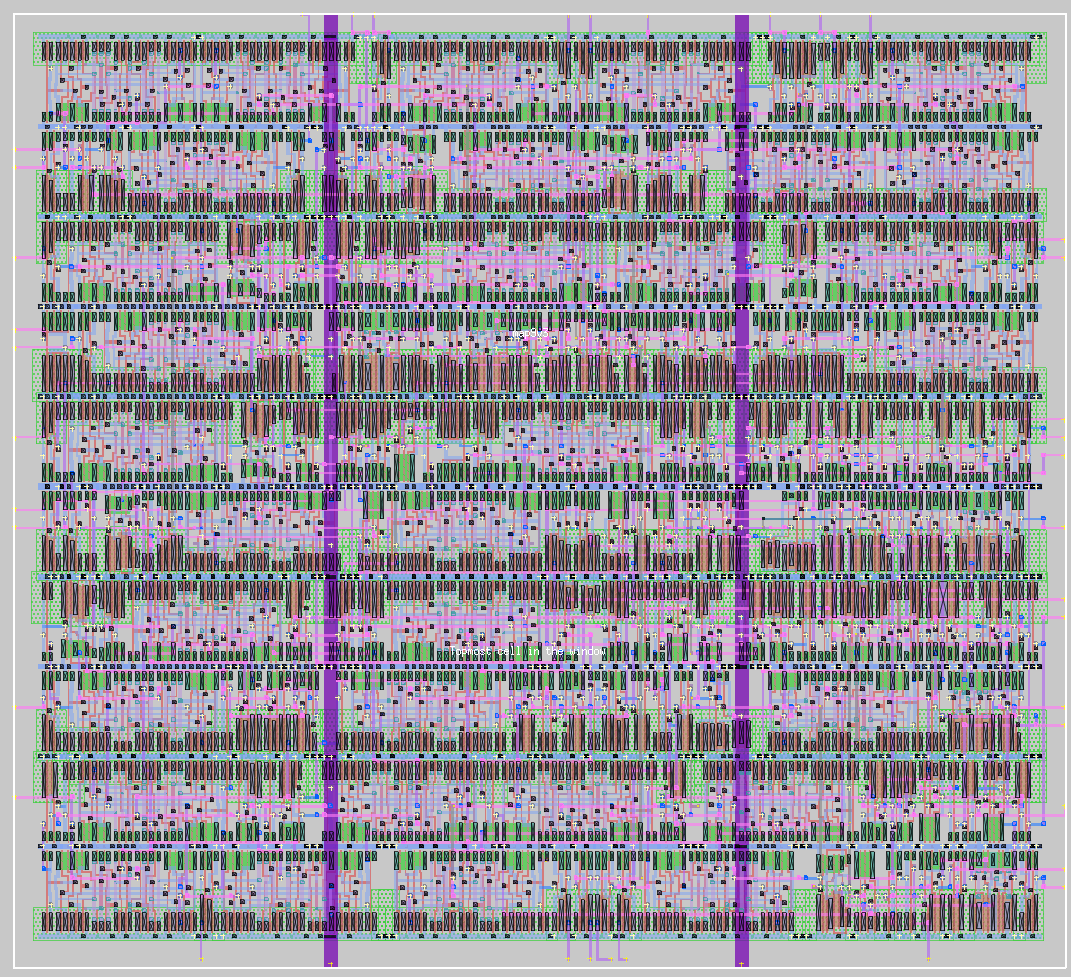
The user settings for "Cleanup" is the option "Purge:". This is always unchecked by default, and never remains checked after a cleanup run. If checked, then "Cleanup" does a destructive clean of all the directories, removing all files except the verilog source file and the project setup files (this means all options chosen during the synthesis flow are remembered).
Although "Cleanup" is the last step and therefore cannot be run until all other steps have completed, if "Purge:" is checked, the Cleanup step can be run at any time, resetting the project back to the beginning.
Simulating the Design
Generally, simulation is not considered to be part of the synthesis flow, although you will certainly want to have verified the design through simulation of the verilog before synthesis. A combination of simulation of the verilog, layout verification through LVS, and post-route timing analysis will suffice to prove the accuracy of the final GDS mask data.There are several ways to simulate the design, including simulation directly on the extracted layout netlist. These simulation techniques are detailed in the command-line version of the qflow tutorial, found here.
Pin Placement Hints
Creating pin hints for the placement can be a complicated task, particularly if there are many pins and they need to be arranged in vectors. The "Arrange Pins" button in the Placement Settings brings up a window with a UI for creating groups of pins and assigning them positions around the layout.Underneath the workings of the GUI, pin hints are kept in a file with the extension ".cel2". This is described in detail in the command-line version of the tutorial as well as in the original documentation for the TimberWolf (graywolf) placement tool. In many cases it may be easier for the experienced user to create the .cel2 file by hand rather than use the UI.
By default, no pin hints are given to the placement. The qflow "Pin Manger" UI window looks like the following on startup:
All the pins of the design are located on the left hand side under the heading "unassigned".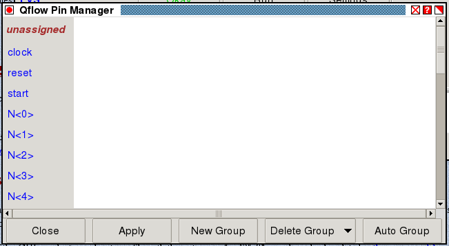
The goal of the pin manager is to make sure that pins are grouped by function or vector index and will be placed in the approximate position on the border of the layout where it needs to go according to (some unspecified) floorplan.
The best way to start is to use the "Auto Group" button, which will find all the vector bits in the design and group them into vectors. This is the result of "Auto Group" on the tutorial design:
Those pins that are not bits of a vector remain at the top under the blanket group "unassigned". The rest have been put into groups. Let's look at what options are available for a group.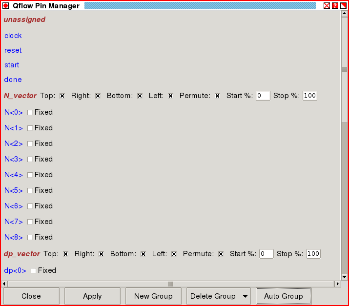
First, there's the group header, which describes where around the layout the signals in the group will be physically placed. There are four choices: Top, Right, Bottom, and Left, but they need not be mutually exclusive. If you select Right and Left but not Top and Bottom, then pins in this group may appear either on the left or right sides of the layout but never on the top and bottom.
In addition to choosing which side or sides the pins of the group may be placed on, there is an additional constraint "Start %" and "Stop %". This specifies the portion of the selected border where pins may be placed. For example, if "Top" is selected along with "Start %" 0 and "Stop %" 50, then pins will be restricted to the left hand half of the top edge of the layout.
After the group header is a list of the pins in the group. These may be specified in any order. If "Fixed" is selected for any signal, then the placement of that signal is fixed with respect to the group. That is, if the second signal of the group is marked "Fixed" in the example above ("Top" selected), then the second signal will always be the second pin along the top counting from the left.
Sometimes it will be helpful to keep the bits of a vector bundled, and in order by index, but you may not care whether the vector goes from high index to low, or from low index to high. In that case, mark all the signals of the vector as "Fixed", but also mark "Permute" in the group header. The "Fixed" setting will keep all the bits in order, but they can be in order from low to high or from high to low.
To arrange the specific order of fixed pins in a group, the pins can be moved around in the pin manager. Simply "grab" the pin with the left mouse button held down. The pin will then show up in inverted color. "Drag" the pin up or down to where you want it to be located relative to other pins. When you release the mouse button, the pin will be "dropped" in that location.
Multiple pins can be moved at a time. Use the right mouse button to click on a number of different signals to highlight them. Then use the left mouse button grab as described above to move the whole group to a different location. Note that while dragging a signal or group of signals, the mouse wheel can be used to scroll up and down while the left mouse button is still held down.
Finally, in addition to the "Auto Group", groups can be individually created or deleted one by one using the "New Group" and "Delete Group" buttons. For a new group, you will be asked to type in the name of the group (which can be any arbitrary text, like "Controls" or "Write_Data" or "Input_Output". . . just make sure the names do not contain spaces). The group will be created as an empty group, and you can add signals to the group by dragging them into the group as described above. The "Delete Group" button is a drop-down menu, so you can select from among the existing groups which one to remove. When a group is removed, its signals are placed back in the "unassigned" group (consequently, deleting the "unassigned" group does nothing).
It is not necessary to assign all pins. Any pins left unassigned will just be placed where the wire length is minimized between the core of the layout and each pin. Remember that it is very easy to over-constrain the pins on a design. So as a general guideline, don't fix pin placements unless you need to. Run the placement step once to to see where the pins end up, and then constrain only what's necessary to match the needs of the floorplan. It is also a good idea to run both placement and routing once before applying pin constraints. That way, it will be very clear if the routing is failing due to pins being over-constrained.
The last step is to apply the constraints by clicking on "Apply", which writes a file with the ".cel2" extension, and then re-run the placement step with the new constraints. There are more options available to the graywolf placement tool than are represented by the pin placement GUI. These can be found in the graywolf documentation. The ".cel2" file is just part of the ".cel" file format; qflow has divided the ".cel" file into a part that is predetermined by the synthesis, and a part (the ".cel2" file) that contains things that are under user control. You may create and hand-edit your own ".cel2" file in the layout directory to apply any constraints known to graywolf. Just make sure that if you have hand-edited a ".cel2" file, you don't hit "Apply" in the pin manager again, or your changes will get overwritten.
Synthesis Flow General Remarks
There are many reasons why synthesis may fail. As mentioned above, when working with a new technology, there are many aspects of the technology setup that can cause failure. Assuming that the technology files are correct, then synthesis failures usually come down to just a small set of problems:Of course, there are always one-off unexpected circumstances, and it is a goal of qflow to provide enough flexibility to deal with them. Solutions, however, may require delving deeply in the documentation, and may not be available in the GUI. Keep in mind that the GUI is merely a convenience, and qflow can be run from the command line when needed, and normally this should not prevent the use of the GUI at other times.
- The design is too dense.
- Designs with lots of combinational logic have dense clusters of pins, and routing can get very congested in these areas, causing routing to fail. The solution is almost always to decrease the density of the design, under "Placement Settings". Area is always a concern, so take the time to run several trials at different initial density, and choose the highest density that results in successful routing.
- There are not enough route layers
- The larger a design is, the more routing layers are needed to route it properly. Trying to route a microprocessor-scale design with just four layers (or worse, three) will almost certainly result in failure. Choose a technology with enough routing resources for the job.
- Pins are over-constrained
- If routing fails and it is clear from looking at the layout that pins are all clustered together in one corner, for example, it is very likely that the pins had too many constraints applied. Don't fix so many pins, and maybe allow pins on more sides. Don't use the percentage length constraint ("Start %" and "Stop %") unless absolutely needed.

email: 
Last updated: October 28, 2025 at 9:47am