Microfabrication Lab Project Report:
A Simple CMOS Pressure Sensor
Typical applications of integrated pressure sensors include microphones, biomedical instrumentation ( e.g., blood and fluid pressure), vacuum sensing, wind-tunnel model instrumentation, automobile power and acceleration measurement, and even household electronics [3].
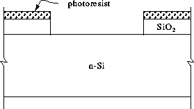
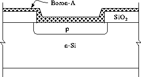
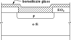
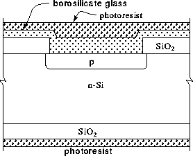
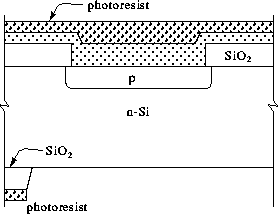
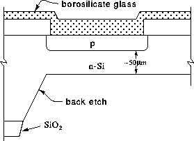
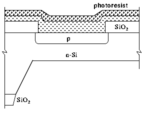
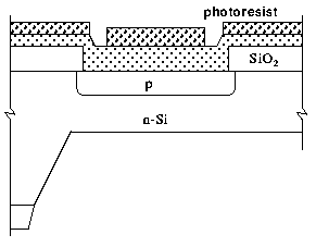
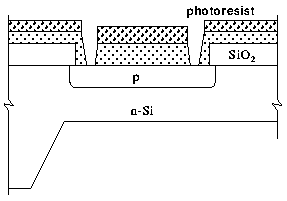
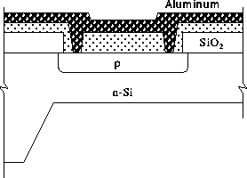
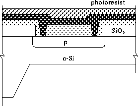
There are a number of ways to go about designing and building an integrated sensor. The most common and inexpensive type, which is the type built for this project, is based on the piezoresistive effect, which is described in detail below. Piezoresitors can be made of doped silicon or polysilicon. Polysilicon has better stability, avoids time- and temperature-variant p-n junctions, and can be used in operating temperatures up to 200°C [1]. All mechanical sensors are based on material changes caused by stress placed on a membrane or other flexible element. On the submillimeter scale of integrated devices, materials like silicon show very little or no fatigue, which is apparently a macroscale phenomenon. Thus integrated sensors can be flexed indefinitely, and have a long lifetime.
In addition to sensors based on the piezoresistive effect, there also exist high-precision sensors based on capacitive effect. A membrane is also used, with one plate of a capacitor mounted on the membrane and the other plate suspended above it, usually fabricated on a relatively inflexible material such as Pyrex glass. The deflection of the membrane changes the distance between the plates and thus changes the capacitance. Capacitors tend to be much less temperature and time variant than piezoresistors. Output of capacitive sensors is highly appropriate for switched-cap circuit design [2].
Other mechanical sensors are based on micromachining techniques. Silicon reed oscillators are formed from a millimeter-scale paddle suspended by a thin silicon bridge, which is caused to oscillate. The amplitude of the vibrations are highly sensitive to pressure changes, and make a good sensor for measuring vacuums in the 10e-2 to 10e5 Pa range. Another kind of vacuum sensor is made from a micromachined floating membrane [1].
When standard or modified CMOS or bipolar processes are used in order to fabricate the sensor, signal processing can be done at the source. On-chip amplification of the signal is the first necessary step to ensure minimizing the effect of noise on the output. On-chip circuitry is also necessary in a high-quality system to compensate for temperature variation. Temperature-dependent behavior is seen as the limiting factor in integrated sensors. Bandgap reference circuits are designed which have a negative temperature coefficient. This is added to the output to compensate for the positive temperature coefficient of the sensor. The voltage reference can either be designed by circuit and material analysis to compensate for the expected temperature dependence of the sensor, or it can be made programmable and the chip can be calibrated after manufacturing. High-performance systems often have bandgap references which are tuned after manufacture by laser trimming [1]. This of course adds to the cost of the device.
Early digitization of the signal is another common treatment which eliminates the problem of noise and nonlinear effects between the sensor and the instrument or control system that depends on its output. An alternative to digital output is a frequency-based output such as duty-cycle variation which is also robust in the presence of noise.
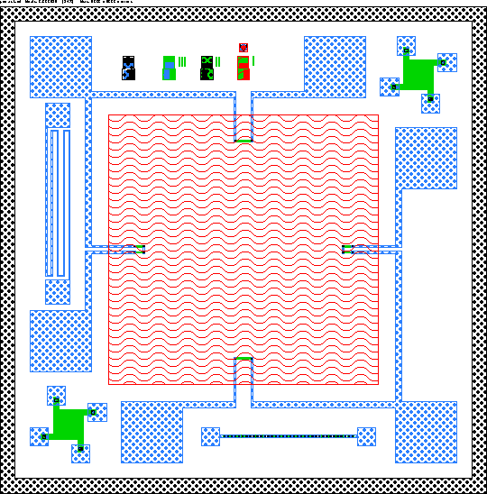
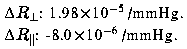
 and
and  are the perpendicular
and parallel components of stress, respectively, and
are the perpendicular
and parallel components of stress, respectively, and
 and
and
 are the
perpendicular and parallel piezoresistive
coefficients. The coefficients are functions of temperature and
doping concentration. The stresses are proportional to pressure
and to the the square of the ratio
are the
perpendicular and parallel piezoresistive
coefficients. The coefficients are functions of temperature and
doping concentration. The stresses are proportional to pressure
and to the the square of the ratio  / h
where h is the thickness of the membrane and
is the distance from the membrane center to the edge [5].
/ h
where h is the thickness of the membrane and
is the distance from the membrane center to the edge [5]. Sensors are sometimes designed using finite element analysis or other precision simulation to find membrane and resistor shapes and configurations which maximize this sensitivity.
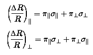
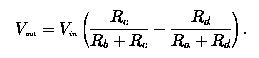
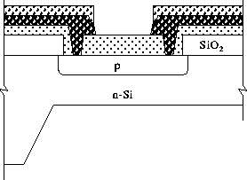
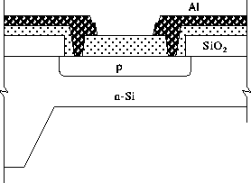
About the simplest sensor circuit that can be built using piezoresistors is the Wheatstone bridge, shown below.
The bridge is made of four piezoresistors
located on the four edges of the sensor membrane, close to the edges where the
stress is greatest when vertical pressure is applied to the center (or uniformly
across) the membrane. Two of the resistors are positioned parallel to the
direction of the stress, and their resistance increases with pressure. The
other two resistors are oriented perpendicual to the direction of the stress,
and their resistance decreases with pressure. This configuration is shown in
the figure below. The parallel resistors are made as two resistors in series in
order to maximize sensitvity, which is a decreasing function of distance
from the edge of the membrane, while keeping the absolute resistance
the same as the perpendicularly-oriented resistors.
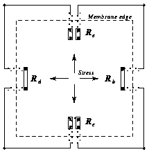
 and
and  are oriented parallel to the stress, and resistors
 and
and  are oriented
perpendicular to it. Thus when the resistance of
increases and decreases,
the output increases. This is the configuration of our
fabricated sensor, with the resistor ends leading to bonding pads.
Configuration of the bridge and signal amplification are all off-chip, to
reduce the number of steps in the process and make is feasible for the
project to be completed by untrained students in one semester.
are oriented
perpendicular to it. Thus when the resistance of
increases and decreases,
the output increases. This is the configuration of our
fabricated sensor, with the resistor ends leading to bonding pads.
Configuration of the bridge and signal amplification are all off-chip, to
reduce the number of steps in the process and make is feasible for the
project to be completed by untrained students in one semester.
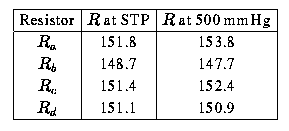
 .
The average standard deviation for resistors around the same membrane was
2.56 ,
but the standard deviation for all resistors was
11.86 .
.
The average standard deviation for resistors around the same membrane was
2.56 ,
but the standard deviation for all resistors was
11.86 . Test structures on the chip were analyzed with the following results:
/ .
/.
.
/.
 to provide a gain of approximately 100.
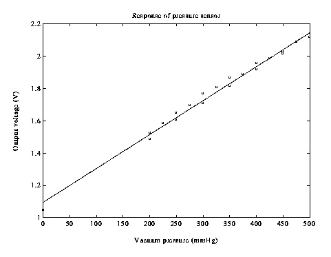
Input was
2.32 V AC at about 100 Hz. Output was measured with the back of the
mounted chip attached to a vacuum pump capable of pressures in the range
50-500 mmHg. Settling time of the response was quite large, possibly
due to the unconnected substrate (which was possibly connected to all of
the resistors through the contacts, which had an extreme amount of
undercut due to overetching), and probably also due to temperature
effects at the resistors heat and cool in response to current flow
in the circuit. Measurements are not entirely accurate
due to the impatience of the observer. Measurements tended to be lower
when read as the vacuum pressure was lowered from 500 mmHg to zero,
and higher when read as the vacuum pressure was raised from zero to
500 mmHg. Due to this and the jitter of the vacuum pump, no attempt
will be made to assess the linearity of the system, other than to
note that it looks reasonable.
to provide a gain of approximately 100.
Input was
2.32 V AC at about 100 Hz. Output was measured with the back of the
mounted chip attached to a vacuum pump capable of pressures in the range
50-500 mmHg. Settling time of the response was quite large, possibly
due to the unconnected substrate (which was possibly connected to all of
the resistors through the contacts, which had an extreme amount of
undercut due to overetching), and probably also due to temperature
effects at the resistors heat and cool in response to current flow
in the circuit. Measurements are not entirely accurate
due to the impatience of the observer. Measurements tended to be lower
when read as the vacuum pressure was lowered from 500 mmHg to zero,
and higher when read as the vacuum pressure was raised from zero to
500 mmHg. Due to this and the jitter of the vacuum pump, no attempt
will be made to assess the linearity of the system, other than to
note that it looks reasonable. Output AC voltage of the system was measured with a Keithly multimeter. The amplifier frequency response was measured in the context of the entire system and had a bandwidth of 30 kHz.
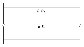
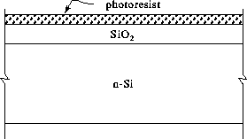
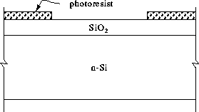
The capacitive pressure sensor is built with a standard CMOS 3 µm n-well process. This is a useful property since the chip can be sent off to any high-quality commercial or institutional lab and postprocessed to create the membrane (obviously the point of our lab was to be hands-on through the entire process). For feature-size comparison, our smallest features were on a 20 µm scale.
The capacitive sensor features a membrane ``bossed'' on the underside, which means the membrane itself forms a square, with the middle of the membrane being the same thickness as the rest of the wafer. This increases linearity of the capacitor by ensuring that the capacitive plates, which are situated over the boss, are flat and move without bending relative to the top plate.
The top plate is formed on Pyrex glass etched to form support columns to hold the capacitor top plate at the proper distance from the bottom. The metal top plate is deposited directly onto the glass, and the glass structure is bonded anodically to the chip. Chip circuitry features a programmable voltage reference and a switched-cap amplifier. Output is a voltage, which makes it easier to compare the performance to that of our chip.
The standard CMOS process involves about 7 or 8 mask steps, and the chip requires one additional mask to define the bossed membrane, and two mask steps are required to etch and metallize the Pyrex glass. This is a total of at least 10 masks for fabrication, compared to our four masks.
Nonlinearity of the chip output voltage was confined to 0.4% over the operating range of 0 to 30 kPa, with an output of 1.0 V to 5.0 V over that range. Note that we did not attempt to find an upper limit of pressure for our sensor, but it is doubtful that it should be operated much above our test limit of 500 Pa. The capacitor pressure sensor therefore has an operating range which is orders of magnitude larger than that of our chip.
Sensitivity for the capacitive sensor is measured as change in capacitance per unit pressure. The capacitor has temperature-dependent offsets and sensitivity which, although not as severe as temperature dependencies in a resistor, can be reduced by the bandgap reference circuit. Due to limited time and equipment, I did not attempt to characterize the temperature dependence of our circuit.
I have very few recommendations for future work; a few things are obvious necessities such as a substrate contact somewhere on the chip, and remaking the mask for which there were no large-scale alignment bars. If the knowledge and experience gained from this year makes next year's project run smoother and faster, then it would probably be well worth the while to add a passivation layer and an extra mask step for contact cuts. It would also be helpful if a better method existed for aligning the back side of the wafer to the front, although it appears that I was the only person to suffer a serious misalignment problem, the source of which is not known to me. One problem with misalignment of the back is that it is virtually impossible to detect the misalignment until the chip is diced up.
Hardcopy (PostScript) of this project report: sensor.ps
![]() Back to my home page. . .
Back to my home page. . .
![]()
| email: | 
|