Our proposed analog module architecture is intended for implementation in a CMOS fabrication technology featuring antifuse (one-time programmable) interconnections. Processes with antifuse capability are digital processes used by the FPGA industry, some of which meet the stringent requirements of radiation tolerance for spaceflight applications. However, they are not well suited to traditional analog circuit design, and so necessitate careful consideration of the analog module design and architecture. Fortunately, this aspect of analog design has been a primary focus of research in recent years due to the wide availability of digital processes and the shrinking availability of dedicated analog processes. This research has produced, for instance, a wide variety of designs for CMOS operational amplifiers maintaining a wide dynamic range while constrained by a low power supply voltage, and designs having good power supply rejection (PSRR), an important consideration in an FPMA architecture where noise from the digital modules will invariably couple into the analog modules.
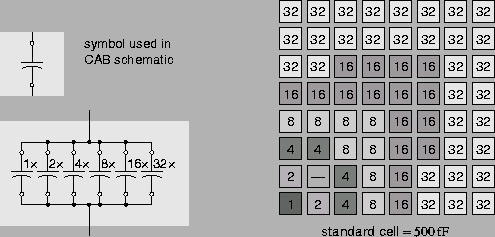
A major constraint of analog VLSI design in a digital process is the requirement for linear capacitors. Field-programmability adds the constraint that fabricated capacitors must have a large capacitance per unit area, so that a sufficient number of programmable capacitor arrays (PCAs) will fit on a single chip of area comparable to standard FPGAs. Capacitors add in parallel, so a PCA with 6 bits of precision is made of 63 equal parts (see Figure 1), each of which must have a capacitance significantly larger than the parasitic capacitances associated with the substrate and the interconnect. This accounts for the fact that PCAs occupy the largest amount of area on an FPAA or FPMA.
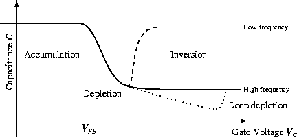
Some analog fabrication processes feature two layers of polysilicon for the purpose of creating linear capacitors. Digital processes usually lack this feature, and often the ``traditional'' metal-polysilicon structure has such low capacitance per unit area that it requires far more die area than can be practically allocated to capacitor arrays. The capacitance associated with the polysilicon-diffusion interface of MOS transistors is typically the largest interlayer capacitance available in a process, but is nonlinear as a function of both voltage and frequency, as shown in Figure 2 [2]. When operated in the accumulation mode, the capacitance is both linear and maximum. However, around the transistor's threshold voltage, the capacitance drops due to capacitive division across the transistor channel.
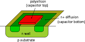
Fortunately, there are several methods available to alleviate the nonlinearity problem [3]. The structure of Figure 3 is one which uses diffusion of the same carrier type as the well surrounding to create the capacitor bottom. This MOS structure, which cannot be used as a transistor, displays the same nonlinear capacitive behavior as the graph of Figure 2, but shifted to the right, which increases the voltage range in which the device operates in the accumulation mode.
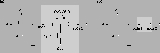
The design solution of Figure 4 [3] is one which can be used when an analog switched-capacitor design requires a voltage across a MOS capacitor large enough to take the device out of accumulation mode and into the region of nonlinear capacitance. Because switched-capacitor designs require resetting the voltage across capacitors to reference values during a portion of the clock cycle, two capacitors can be placed back-to-back with the voltage between them set, during the refresh period, to a bias value ensuring accumulation-mode operation. During the remainder of the cycle, the shared node is decoupled from the bias, and the two capacitors behave like a single linear capacitor.
 |
Last updated: October 13, 1999 at 3:00pm