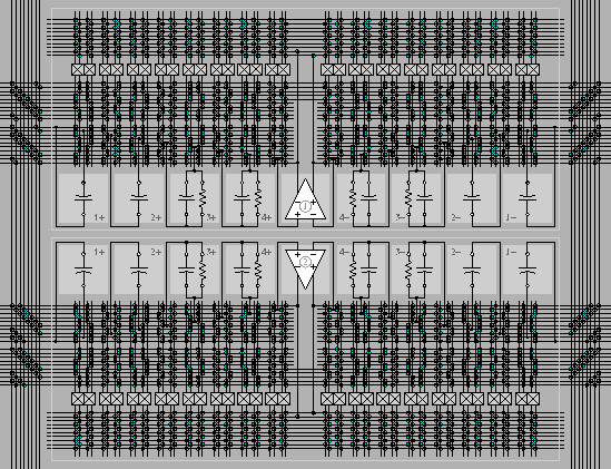
In an attempt to answer questions about the viability of an FPAA using antifuse technology in a digital process, we have designed a test structure to be fabricated on the Actel RT-SX process, incorporating twelve analog modules in a 3 x 4 array, which will allow us to test both continuous-time and switched-capacitor designs of numerous standard spaceflight applications, including pulse shaping, analog-to-digital and digital-to-analog conversion, modulators, oscillators, and filters.
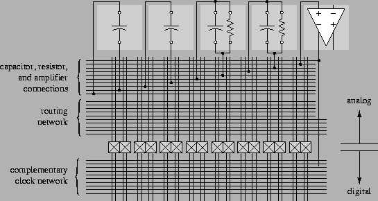
The design of a single block incorporates circuit components as resources which can be connected into the circuit individually using antifuses. When unprogrammed, the resources are decoupled from the circuit except through the small antifuse capacitance. Our FPAA analog module design contains the following resources:
The operational amplifier is a two-stage differential design for a digital process published in Yoshizawa, et al. [3], modified as necessary to meet design rules and maintain stability over the range of output loading capacitances possible with programming of the PCA. A continuous-time, rather than switched-capacitor, circuit performs common-mode feedback (CMFB); it consumes more power but allows the amplifier to be used in continuous-time as well as switched-capacitor circuit configurations. In a production version it would be desirable to reprogram the amplifier circuit for optimum performance under varying conditions, such as speed for use as a comparator.
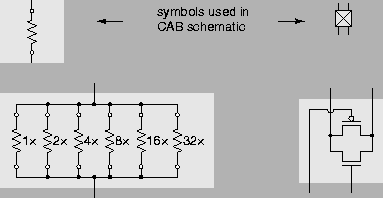
Figure 1 shows the programmable capacitor array schematic
used. Figure 5 shows the remainder of the resources,
 |
Last updated: October 13, 1999 at 3:06pm